Bonding structure, bonding method and packaging box body containing bonding structure

A technology of bonding structure and packaging box, which is applied in the direction of assembling printed circuits with electrical components, printed circuits connected with non-printed electrical components, and parts of chassis/cabinet/drawer, etc., which can solve the horizontal displacement of quantum chips. , not firm, poor thermal contact and other problems, to achieve the effect of improving space utilization, chip mounting firm, and improving bonding strength

Pending Publication Date: 2019-11-12
UNIV OF SCI & TECH OF CHINA
View PDF0 Cites 0 Cited by
  • Summary
  • Abstract
  • Description
  • Claims
  • Application Information

AI Technical Summary

Problems solved by technology

[0004] The problem is that the existing installation method puts the quantum chip into the packaging sample box from top to bottom, puts it on the PCB board, and glues it to the PCB board, which is prone to uneven and weak bonding, and may Cause horizontal displacement, vibration and poor thermal contact with the base of the quantum chip
[0005] Moreover, in the process of the quantum chip from room temperature to low temperature, thermal expansion and contraction will occur, which may lead to poor contact, so it is very necessary to optimize the connection method

Method used


Image

  • Bonding structure, bonding method and packaging box body containing bonding structure
  • Bonding structure, bonding method and packaging box body containing bonding structure
  • Bonding structure, bonding method and packaging box body containing bonding structure

Examples


no. 1 example

[0048] In a first exemplary embodiment of the present disclosure, there is provided a bonding structure.

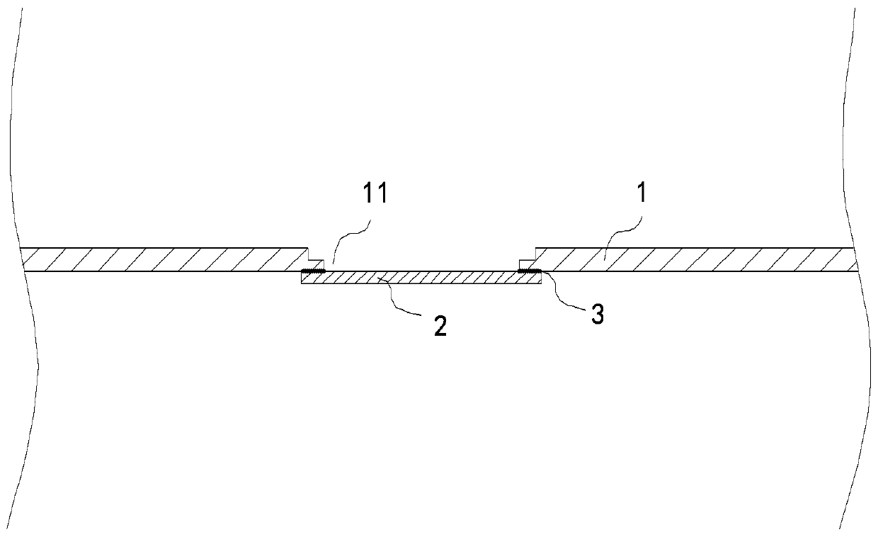
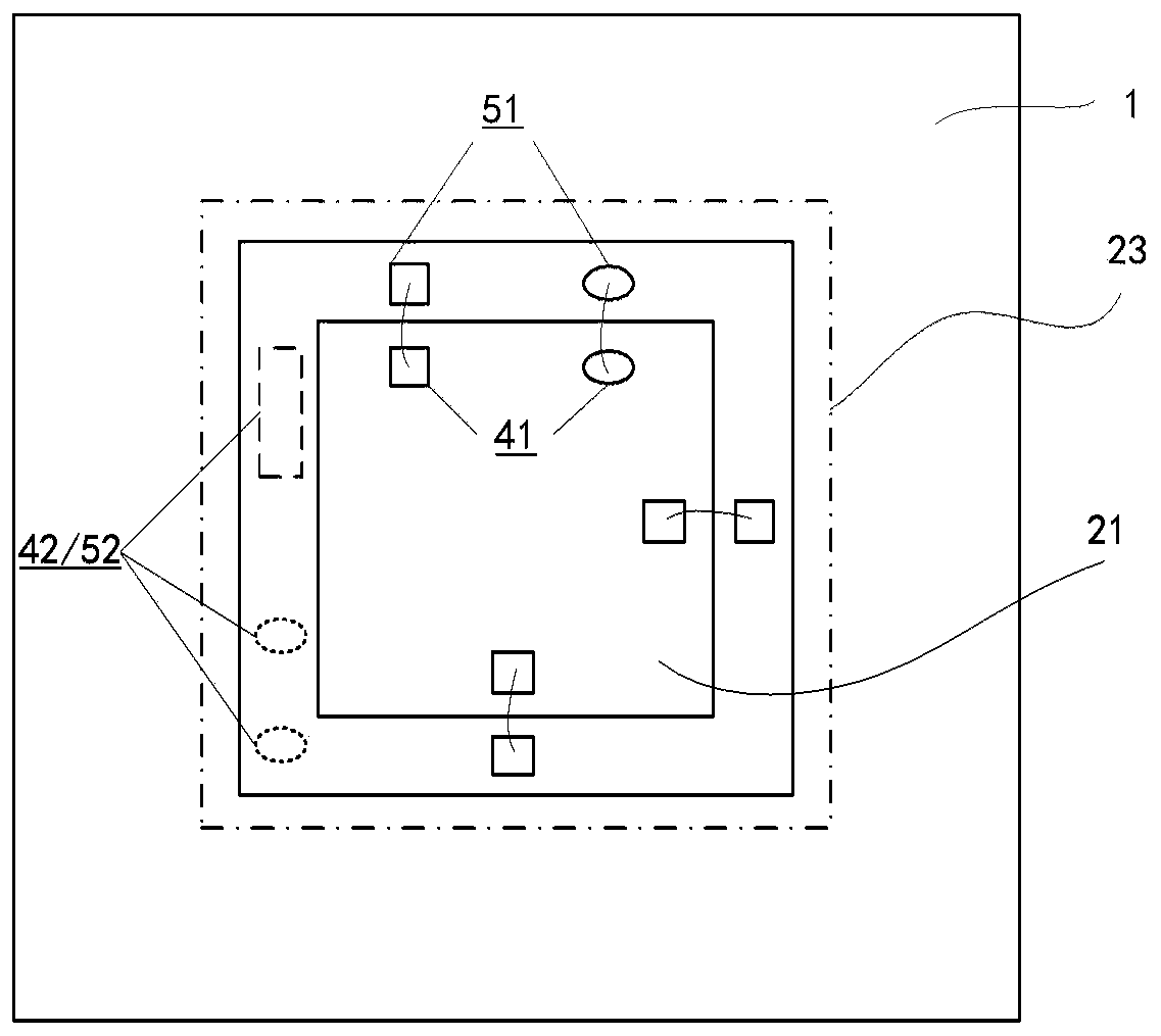
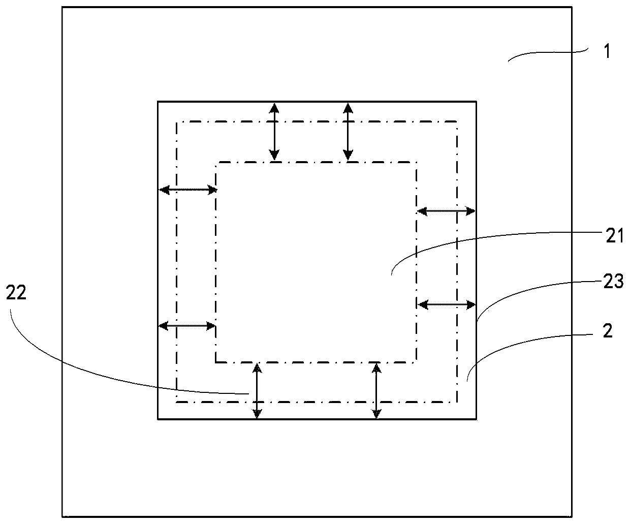
[0049] figure 1 It is a schematic cross-sectional structure diagram of a bonding structure according to an embodiment of the present disclosure. figure 2 It is a front top view of a bonding structure according to an embodiment of the present disclosure. image 3 It is a top view of the back side of the bonding structure shown according to an embodiment of the present disclosure. image 3 A thicker black line is used to indicate the back contact area 3 between the quantum chip 2 and the PCB board.

[0050] refer to Figure 1-Figure 3 As shown, the bonding structure of the present disclosure includes: a quantum chip 2; a PCB board 1 for bonding with the quantum chip 2, the PCB board 1 is provided with an opening 11, and the length and width of the opening 11 are The size or radial size is smaller than the corresponding size of the quantum chip 2; wherein, the quantum c...

no. 2 example

[0064] In a second exemplary embodiment of the present disclosure, a bonding method is provided.

[0065] In this embodiment, the bonding method includes:

[0066] Step S21: preparing a quantum chip;

[0067] In this embodiment, the shape of the quantum chip is a square (top view), and its size means side length. In other embodiments, the quantum chip can also be in other shapes, such as circular, polygonal or elliptical.

[0068] Step S22: Prepare a PCB board, the PCB board is provided with an opening, and the length, width or radial dimension of the opening is smaller than the corresponding size of the quantum chip;

[0069] In this embodiment, the opening of the PCB board corresponds to a rectangle. Of course, it can also be a circular, polygonal or other shaped opening, as long as the length, width or radial dimension of the opening is smaller than the corresponding size of the quantum chip. In other words, the quantum chip is placed close to the back of the PCB board f...


PUM


Abstract

Disclosed are a bonding structure, a bonding method and a packaging box body containing the bonding structure; the bonding structure comprises a quantum chip and a PCB; the PCB is used for being bonded with the quantum chip, an opening is formed in the PCB, and the length, the width or the diameter size of the opening are smaller than the corresponding size of the quantum chip; the quantum chip islocated below the opening of the PCB and makes contact with the PCB; the upper surface of the first part of the quantum chip is exposed through the opening, and the upper surface of the second part is shielded by the PCB on the edge of the opening. The size of the opening is smaller than that of the quantum chip, so that the quantum chip can be in additional contact with the PCB from the back surface of the PCB, the area where the quantum chip makes contact with the PCB can be used for grounding or signal connection, the wiring area on the front surface of the PCB is effectively saved, and the overall bonding strength is improved; and in addition, the phenomenon that the chip and a sample box base are not firmly combined and the heat contact between the chip and the base is poor during installation when a chip is placed from the front surface of the PCB can be avoided.

Description

technical field [0001] The disclosure belongs to the technical field of quantum chip packaging, and relates to a bonding structure, a bonding method and a packaging box containing the bonding structure, especially a bonding structure that can be used in an extremely low temperature environment (for example, less than 10mK) and Its bonding method, and the packaging box containing the bonding structure. Background technique [0002] In the implementation of superconducting quantum computing, connecting the quantum processor with peripheral circuits is an indispensable step. The encapsulation box of the superconducting quantum processor is the first-level device connected with the quantum processor. How to connect and fan out the various performance pins of the superconducting quantum processor, and ensure that the interference to the signal performance on the line is minimized has become a design problem in the industry. [0003] In order to realize the input and output of c...

Claims


Application Information

Patent Timeline
Patent Type & Authority Applications(China)
IPC IPC(8): H05K3/32H05K1/18H05K5/02
CPCH05K3/32H05K1/18H05K5/03
Inventor 梁福田邓辉龚明吴玉林彭承志朱晓波潘建伟
Owner UNIV OF SCI & TECH OF CHINA
Why Eureka
Try Eureka