
Eureka
For R&D, Eureka makes reading and utilizing patents & technical documents easy.
Eureka AIR
Designed for self-driven R&D workflows. Generate viable solutions, solve complex R&D challenges, empower your innovation with AI.

Eureka Materials
Designed for material experts only. Revolutionize your material R&D, from search, analyze, to developing new materials.

TechResearch
Generate reliable direction feasibility study reports for your R&D in just a few steps.

TechSeek
Discover and master advanced knowledge NOW. Basics, ideas, possibilities, all at once.

TechMind
As an expert in R&D Theories, TechMind can generates customized viable solutions instantly.

TechRisk
Analyze your overall solution with one click, know your potential R&D risks in advance.

TechMonitor
Get weekly tech updates, stay abreast of the latest tech innovations and key insights.
Semiconductor component packaging method and alignment mold thereof
A packaging method and semiconductor technology, applied in the direction of semiconductor devices, semiconductor/solid-state device manufacturing, electrical components, etc., can solve the problems of inaccurate alignment, derivation, and increased installation costs of light-emitting diodes, and achieve the effect of improving packaging quality
- Summary
- Abstract
- Description
- Claims
- Application Information
AI Technical Summary
Problems solved by technology
Method used
Image

Examples
Embodiment Construction
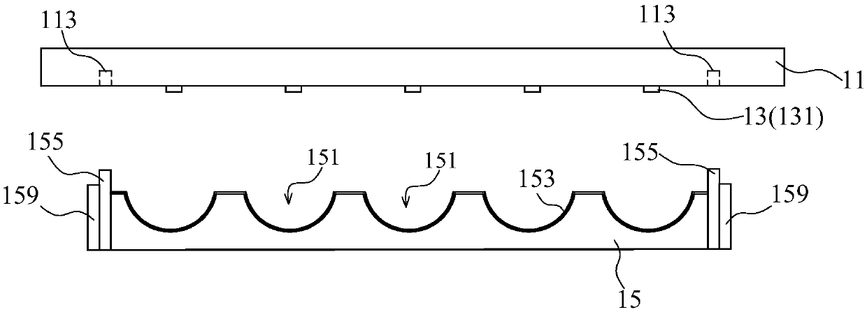
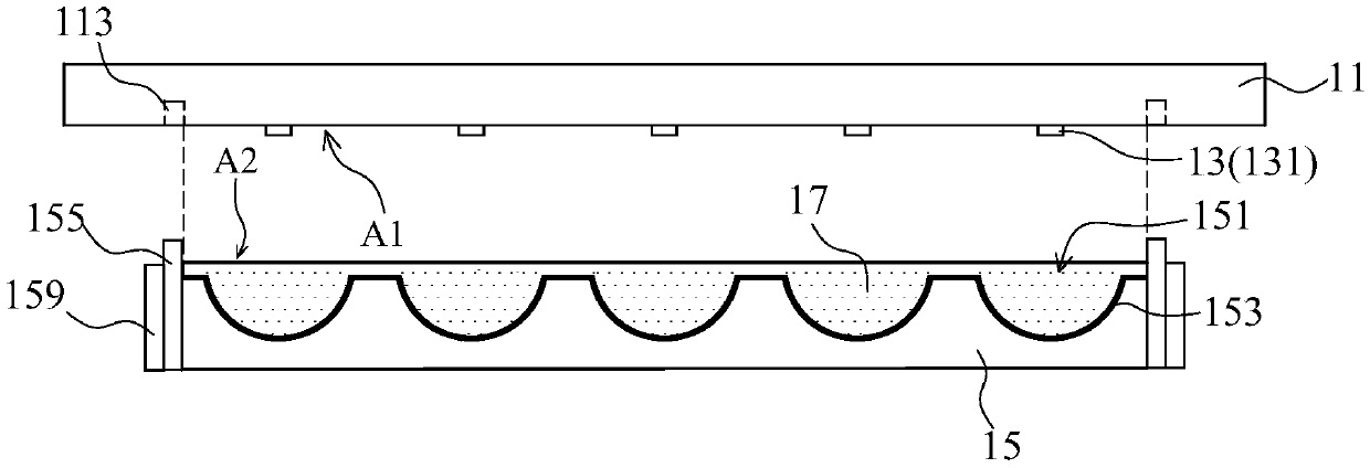
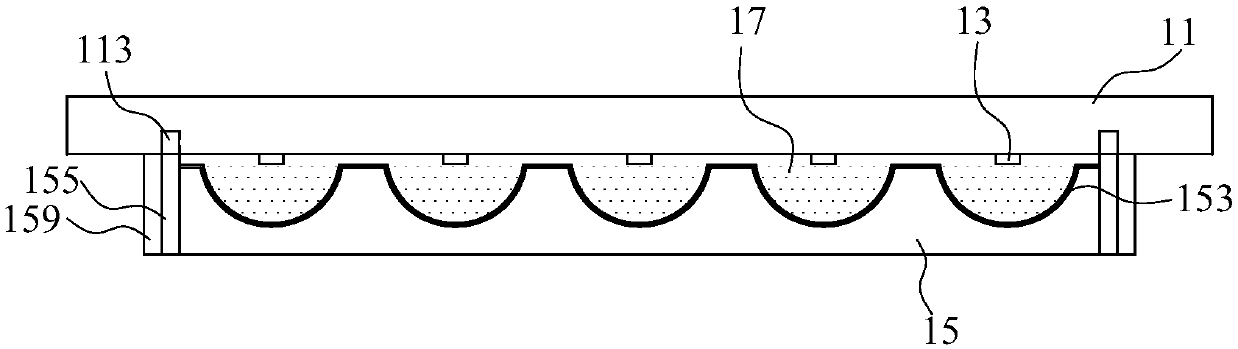
[0031] See Figure 1 to Figure 4 , Respectively are side views of an embodiment of the semiconductor device packaging method of the present invention in each step. As shown in the figure, first, a plurality of semiconductor elements 13 are arranged on a surface of a substrate 11, and a mold 15 is prepared. The mold 15 has a plurality of molding cavities 151, such as figure 1 Shown. The substrate 11 may be a silicon (Si) substrate, alumina (A 2 O 3 ) Substrate, aluminum nitride (AlN) substrate, sapphire substrate, silicon carbide (SiC) substrate, gallium arsenide (GaAs) substrate, glass substrate (Glass), circuit board (PCB) or ceramic substrate.
[0032] Specifically, the semiconductor elements 13 arranged on the surface of the substrate 11 may be arranged in any form, for example, arranged on a surface of the substrate 11 in a matrix. The semiconductor element 13 may be a light-emitting diode die, a semiconductor chip, etc., taking the light-emitting diode die 131 as an example...
PUM
 Abstract
Description
Claims
Application Information
 - R&D Engineer
- R&D Manager
- IP Professional
- Industry Leading Data Capabilities
- Powerful AI technology
- Patent DNA Extraction
Browse by: Latest US Patents, China's latest patents, Technical Efficacy Thesaurus, Application Domain, Technology Topic, Popular Technical Reports.
© 2024 PatSnap. All rights reserved.Legal|Privacy policy|Modern Slavery Act Transparency Statement|Sitemap|About US| Contact US: help@patsnap.com