Large-board fan-out double-sided antenna package structure and preparation method thereof

A packaging structure and double-sided technology, applied in the direction of antenna support/mounting device, antenna, antenna parts, etc., can solve the problems of large board fan-out packaging structure with large warpage, increased production cost, and low production efficiency , to achieve the effects of reasonable packaging structure layout, improved integration performance, and improved production efficiency

Pending Publication Date: 2019-11-15
广东佛智芯微电子技术研究有限公司
View PDF0 Cites 5 Cited by
  • Summary
  • Abstract
  • Description
  • Claims
  • Application Information

AI Technical Summary

Problems solved by technology

[0004] (1) For the large board fan-out packaging structure, due to the large size, the warpage of the large board fan-out packaging structure is relatively large;
[0005] (2) The antenna occupies an additional circuit board area, which increases the volume of the fan-out antenna package structure, resulting in poor product integration and high cost
For various high-tech electronic products, if the antenna is directly fabricated on the surface of the circuit board, and then the antenna and the chip are connected through an electrical connection structure, it means that a larger circuit board is required, so that high-tech electronic products also occupy a relatively large area. Large volume, and will make the transmission line longer, poor performance and high power consumption, which is contrary to people's demand for miniaturization, portability, high performance and low power consumption of high-tech electronic products;
[0006] (3) Only one fan-out antenna package structure is made on one carrier board, and the production efficiency is low, thereby increasing the production cost of the product

Method used


Image

  • Large-board fan-out double-sided antenna package structure and preparation method thereof
  • Large-board fan-out double-sided antenna package structure and preparation method thereof
  • Large-board fan-out double-sided antenna package structure and preparation method thereof

Examples


Embodiment Construction

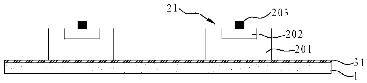
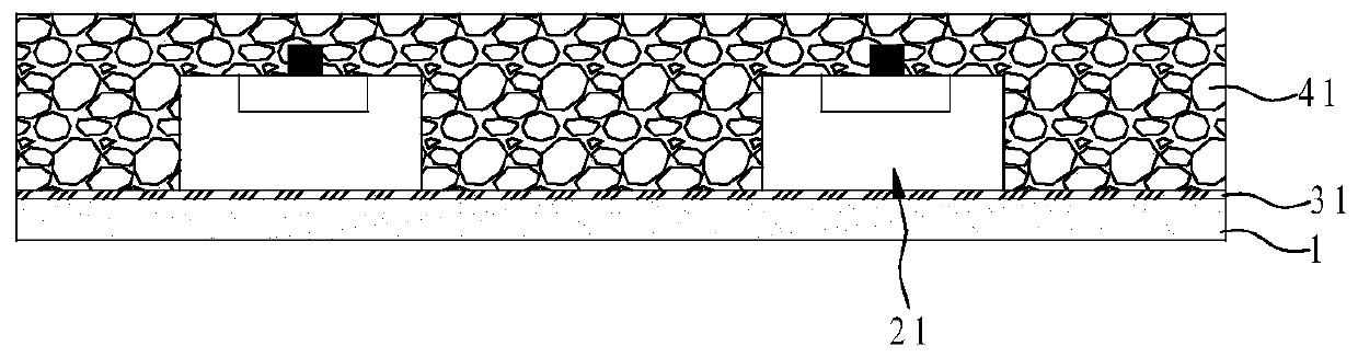
[0087] The technical solutions of the present invention will be further described below in conjunction with the accompanying drawings and through specific implementation methods.

[0088] Wherein, the accompanying drawings are only for illustrative purposes, showing only schematic diagrams, rather than physical drawings, and should not be construed as limitations on this patent; in order to better illustrate the embodiments of the present invention, some parts of the accompanying drawings will be omitted, Enlargement or reduction does not represent the size of the actual product; for those skilled in the art, it is understandable that certain known structures and their descriptions in the drawings may be omitted.

[0089] In the drawings of the embodiments of the present invention, the same or similar symbols correspond to the same or similar components; , "inner", "outer" and other indicated orientations or positional relationships are based on the orientations or positional ...


PUM


Abstract

The invention discloses a large-board fan-out double-sided antenna package structure and a preparation method thereof. The large-board fan-out double-sided antenna package structure includes a carrierplate, a number of semiconductor chips, package layers, transmission layers, wiring layers, antenna layers, solder mask layers and metal bumps. The backs of the semiconductor chips are attached to the two sides of the carrier plate. The package layers are respectively located on the two sides of the carrier plate and cover the semiconductor chips, and the fronts of the semiconductor chips are exposed to the package layers. The transmission layers, the wiring layers and the antenna layers are all located on the package layers. One side of each transmission layer is electrically connected withthe corresponding package layer and the fronts of the corresponding semiconductor chips, and the other side is electrically connected with the corresponding wiring layer and the corresponding antennalayer. Each wiring layer has a pad area and a non-pad area. The solder mask layers are located on the package layers and cover the antenna layers and the non-pad areas. The metal bumps are welded to the pad areas of the wiring layers. The antenna layers occupy small volume, and the package structure is arranged reasonably. The integration performance of the antenna packaging structure and the efficiency of antennas can be improved. Surface warpage will not be caused due to the performance difference of materials. The accuracy, yield and welding stability during production can be guaranteed.

Description

technical field [0001] The invention relates to the technical field of fan-out packaging, in particular to a large-plate fan-out double-sided antenna packaging structure and a preparation method thereof. Background technique [0002] Fan-out packaging is one of the more flexible advanced packaging methods, and it has unique advantages compared with conventional wafer-level packaging. In the fan-out antenna packaging structure, the antenna needs to use multiple functional chip modules to combine the signal transmission and reception. [0003] The traditional method of fan-out antenna packaging structure is: attach a semiconductor chip to one side of the carrier board, and then lead the antenna out through an electrical connection structure, so that the antenna is located on the surface of the circuit board. This approach has the following defects in the actual production and application of the product: [0004] (1) For the large board fan-out packaging structure, due to the...

Claims


Application Information

Patent Timeline
Patent Type & Authority Applications(China)
IPC IPC(8): H01L23/31H01L21/56H01Q1/22
CPCH01L21/56H01L23/3121H01Q1/2283H01L2224/18
Inventor 崔成强姚颍成林挺宇
Owner 广东佛智芯微电子技术研究有限公司
Why Eureka
Try Eureka