Device single-event effect weak point mapping screening device and method

A single event effect and weak point technology, applied in aerospace technology and semiconductor fields, can solve the problem of time and space dynamic synchronization without establishing a joint test simulation device for multiple effects

Active Publication Date: 2019-11-19
NAT SPACE SCI CENT CAS
View PDF7 Cites 8 Cited by
  • Summary
  • Abstract
  • Description
  • Claims
  • Application Information

AI Technical Summary

Problems solved by technology

[0005] The purpose of the present invention is to overcome the defects that the test method in the prior art does not establish a joint test for multiple effects and for the time and space dynamic synchronization between the simulation device and the device under test, so as to provide a method that can perform a single test on the device under test. Time and space dynamic detection device and method during particle lock (SEL), single event transient (SET) and single event upset (SEU), the following Chinese and English abbreviations SEL represent described single event locking, SET represents single event transient, SEU stands for Single Event Upset

Method used


Image

  • Device single-event effect weak point mapping screening device and method
  • Device single-event effect weak point mapping screening device and method
  • Device single-event effect weak point mapping screening device and method

Examples


Embodiment Construction

[0097] The present invention will be described in detail below in conjunction with the accompanying drawings and specific embodiments.

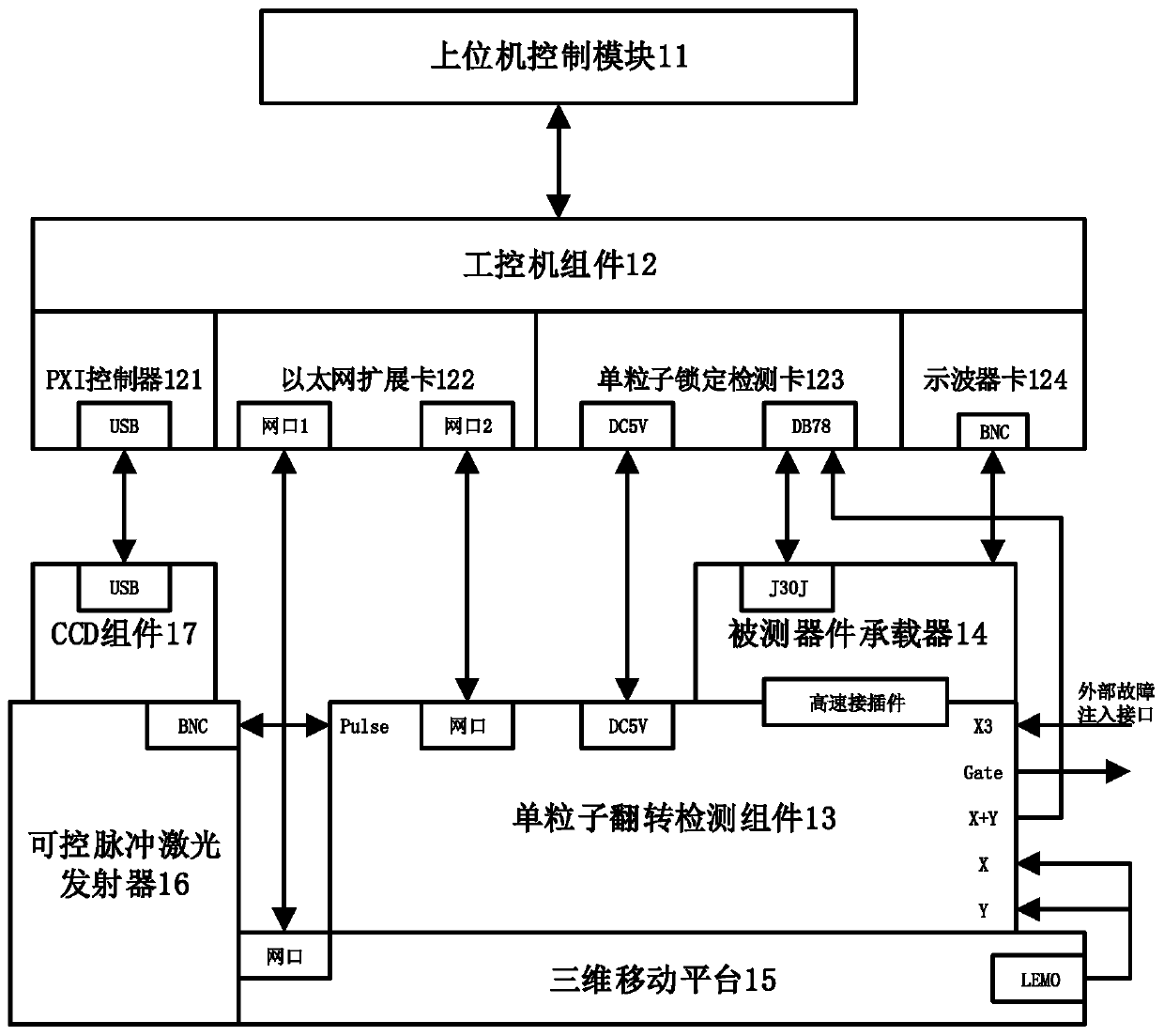
[0098]The present invention proposes a single event effect weak point surveying and screening device, including: a host computer control module 11, an industrial computer component 12, a single event reversal detection component 13, a device under test carrier 14, a three-dimensional mobile platform 15, a controllable pulse Laser emitter 16 and CCD camera 17; Wherein,

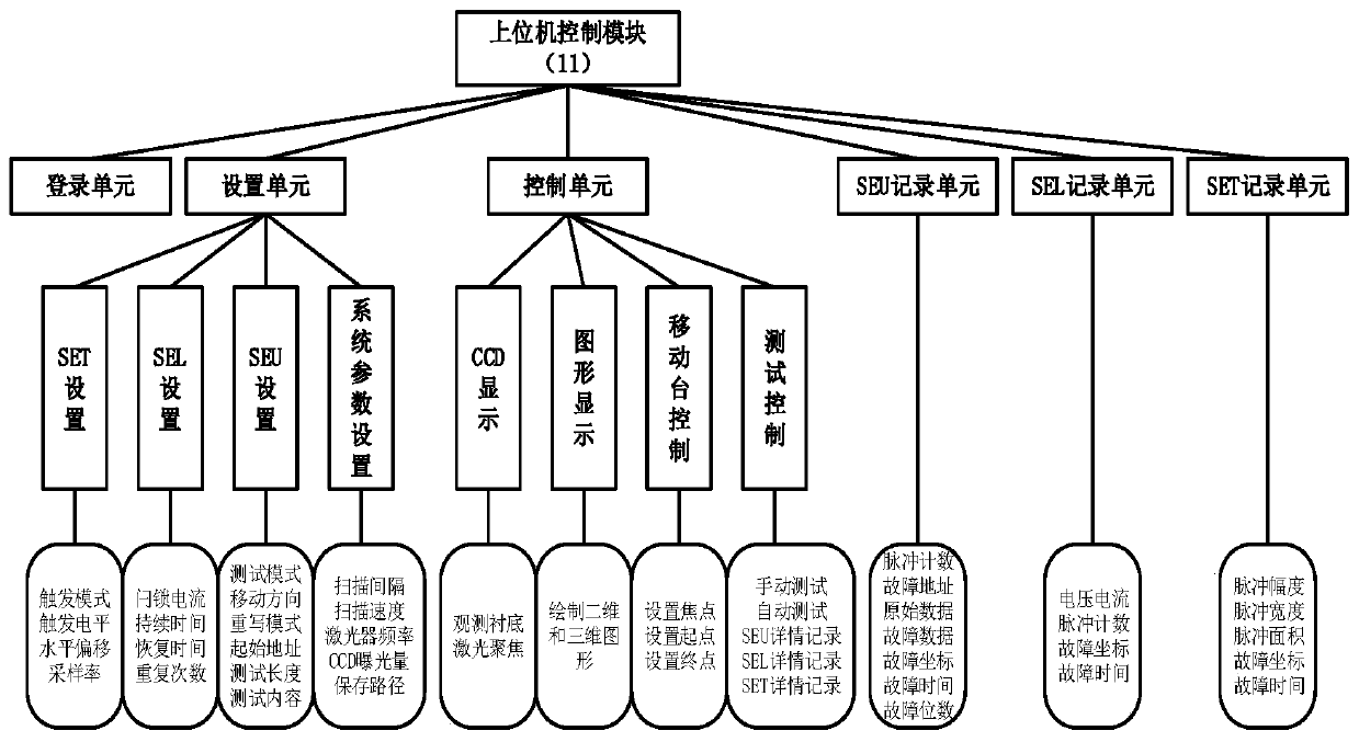
[0099] The upper computer control module 11 is used to realize the control of the movement mode and test mode of the whole device and the display and drawing of fault data;

[0100] Described industrial computer component 12 adopts PXI system to complete system test, and its interior comprises standard PXI controller 121, Ethernet expansion card 122, oscilloscope card 124 and the single event locking detection card 123 of self-developed;

[0101] The single event reversal det...


PUM


Abstract

The invention provides a device single-event effect weak point mapping screening device and method, and the device comprises a host computer control module (11), a single-event flip detection component (13), a tested device loader (14), a three-dimensional mobile platform (15), a controllable pulsed laser emitter (16), a CCD component (17) and an industrial computer component (12), wherein the upper computer control module (11) is configured to send the set moving position interval and test mode parameters to the industrial computer component (12), display and plot according to the fault datacollected by the industrial computer component (12), and obtain the sensitivity and a sensitive area when the tested device has a single-event effect; and the industrial computer component (12) is configured to form a movement control instruction according to the received set parameters, send the instruction to the single-event flip detection component (13) to control the three-dimensional mobileplatform (15), and upload the single-event flip state data and the CCD image to the upper computer control module (11). The invention can perform mapping and discrimination on the physical position and time when the single-event effect of the tested device occurs.

Description

technical field [0001] The invention relates to the fields of aerospace technology and semiconductor technology, in particular to a device and method for mapping and identifying weak points of single event effects of devices. Background technique [0002] Single event effect (Single event effect) refers to the phenomenon that high-energy charged particles generate a large amount of charge in the sensitive area of ​​the device. When particles with sufficient energy are injected into the integrated circuit, due to the ionization effect, the integrated circuit will generate a large number of electron-hole pairs. These sudden excess charges will cause the failure of the semiconductor device, causing the device to store bit flips or logic Level jumps lead to single event upset (single event upset) or single event function interrupt (single event function interrupt), which can cause CMOS devices to generate large currents and cause single event latch-up (single event latch-up). If...

Claims


Application Information

Patent Timeline
Patent Type & Authority Applications(China)
IPC IPC(8): G01R31/265
CPCG01R31/2656
Inventor 朱翔韩建伟李悦马英起陈睿上官士鹏
Owner NAT SPACE SCI CENT CAS
Why Eureka
Try Eureka