
Touch display and manufacturing method of touch display

A touch display and touch electrode technology, applied in the input/output process of instruments, data processing, optics, etc., can solve the problems of insufficient capacitance value of storage capacitors, increase material costs, increase production time, etc., to save production process Steps and the effect of reducing production cost and increasing capacitance value

Active Publication Date: 2019-11-19
HANNSTAR DISPLAY CORPORATION
View PDF4 Cites 13 Cited by
  • Summary
  • Abstract
  • Description
  • Claims
  • Application Information

AI Technical Summary

Problems solved by technology

However, as the size of the pixel shrinks, the overlapping area of ​​the two transparent electrodes used to control the storage capacitor of the display screen in the pixel will also decrease accordingly, resulting in insufficient capacitance value of the storage capacitor, thereby affecting the electrical properties of the storage capacitor and the display screen. Therefore, maintaining or improving the electrical properties of the storage capacitor when the image resolution is improved is an urgent goal for the relevant technical personnel to achieve.
In addition, most of today's touch displays are provided with at least three layers of metal layers, to respectively set the traces electrically connected to the gate of the thin film transistor, the traces electrically connected to the source of the thin film transistor, and the traces electrically connected to the touch electrodes. , but under this structure, its manufacturing process is more complicated, resulting in increased material costs and increased production time, which in turn affects production costs and production capacity

Method used


Image

  • Touch display and manufacturing method of touch display
  • Touch display and manufacturing method of touch display
  • Touch display and manufacturing method of touch display

Examples


Embodiment Construction

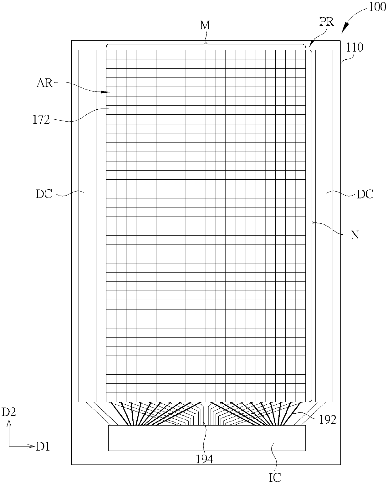
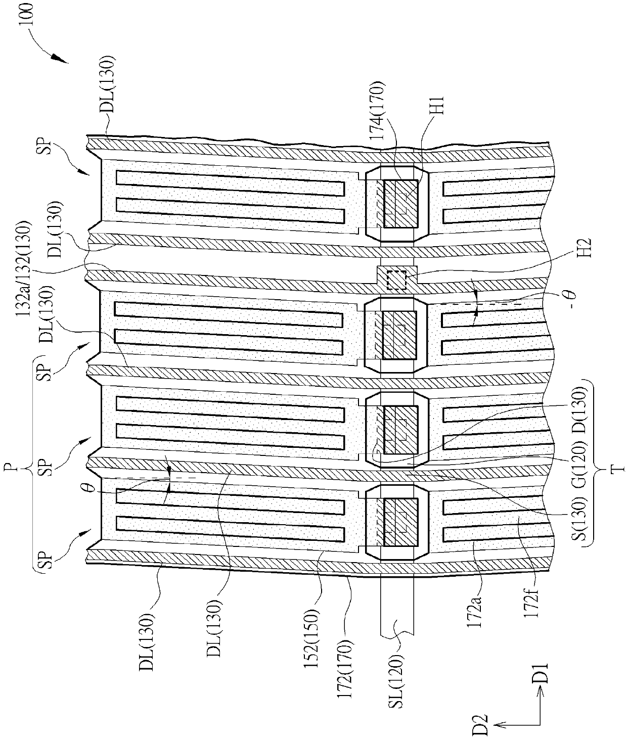
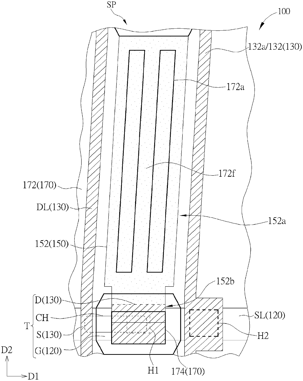
[0085] In order to enable those skilled in the art to further understand the present invention, the preferred embodiments of the present invention are listed below, and the composition and desired effects of the present invention are described in detail with reference to the accompanying drawings. It should be noted that the drawings are all simplified schematic diagrams, therefore, only the components and combinations related to the present invention are shown to provide a clearer description of the basic structure or implementation method of the present invention, and the actual components and layout may be more accurate. for complex. In addition, for the convenience of description, the components shown in the drawings of the present invention are not drawn in proportion to the number, shape, and size of the actual implementation, and the detailed proportions can be adjusted according to design requirements.

[0086] Please refer to figure 1 , figure 1 Shown is a schematic...


PUM


Abstract

The invention discloses a touch display which comprises a substrate, a thin film transistor, a touch signal line, a first insulating layer, a first transparent conducting layer, a second insulating layer, a first connecting hole, a second connecting hole and a second transparent conducting layer. The thin film transistor and the touch signal line are arranged on the substrate. The first insulatinglayer, the first transparent conducting layer and the second insulating layer are sequentially arranged on the thin film transistor and the touch signal line, wherein the first transparent conductinglayer comprises a pixel electrode. The first connecting hole and the second connecting hole are located in the first insulating layer and the second insulating layer, the first connecting hole exposes a part of the pixel electrode and a part of the drain electrode of the thin film transistor, and the second connecting hole exposes a part of the touch signal line. The second transparent conductinglayer is arranged on the second insulating layer and comprises a touch electrode and a connecting electrode, and the connecting electrode and the control electrode extend into the first connecting hole and the second connecting hole respectively and are electrically insulated from each other.

Description

technical field [0001] The invention relates to a touch display and a manufacturing method thereof, in particular to a touch display capable of increasing storage capacitance and a manufacturing method thereof. Background technique [0002] The touch display is composed of two substrates, a plurality of film layers and various electronic components arranged between the two substrates, so as to achieve the functions of displaying images and touch sensing. Due to the characteristics of thin and light appearance, low power consumption and no radiation pollution, the touch display has been widely used in various portable or wearable electronic products such as notebook computers (notebooks), smart phones (smart phones) , watches and car displays, etc., to provide more convenient information transmission and display. [0003] In order to increase the picture resolution of the touch display, the size of pixels in the touch display is generally reduced, so that the number of pixel...

Claims


Application Information

Patent Timeline
Patent Type & Authority Applications(China)
IPC IPC(8): G06F3/041G06F3/044
CPCG06F3/0412G06F3/044G06F2203/04103G06F3/0446G02F1/13338G02F1/136286G02F1/134372G02F1/13606G02F1/134363G02F1/136227G02F1/133345G02F1/136213G02F1/13439G06F3/0445G02F2201/121G02F2201/123G02F1/1368G02F1/136295
Inventor 叶政谚苏国彰
Owner HANNSTAR DISPLAY CORPORATION
Learn More