Separated gate VDMOS device with high channel density and manufacturing method thereof

A technology of separating gates and channels, which is applied in the manufacture of semiconductor/solid-state devices, semiconductor devices, electrical components, etc., can solve the problems of reducing the specific conductance of devices, increase channel density, increase conductive channels, and reduce operating losses. Effect

Inactive Publication Date: 2019-11-22
UNIV OF ELECTRONIC SCI & TECH OF CHINA
View PDF3 Cites 2 Cited by
  • Summary
  • Abstract
  • Description
  • Claims
  • Application Information

AI Technical Summary

Problems solved by technology

The existing split-gate VDMOS device increases the channel density of the device by reducing the width of the mesa, thereby further reducing the specific conductance of the device, but this method is limited by the process capability, which brings new challenges to the device design

Method used


Image

  • Separated gate VDMOS device with high channel density and manufacturing method thereof
  • Separated gate VDMOS device with high channel density and manufacturing method thereof
  • Separated gate VDMOS device with high channel density and manufacturing method thereof

Examples


Embodiment 1

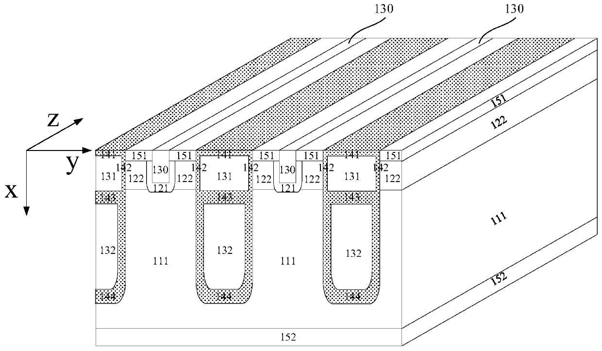
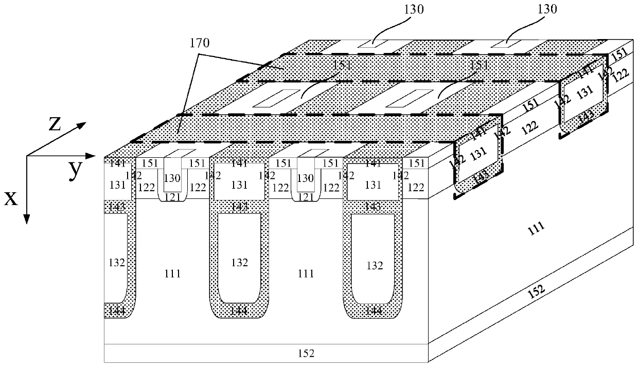
[0044] Such as figure 2 It is the overall structure of the split-gate VDMOS device in Embodiment 1 of the present invention, its cross-sectional view is shown in FIG. 3 , and its top view is shown in FIG. Figure 4 shown, including:

[0045] First conductivity type substrate 152, first conductivity type drift region 111, first conductivity type source contact region 151, second conductivity type well region 122, second conductivity type source terminal contact region 121, source metal contact 130, A first dielectric oxide layer 141, a second dielectric oxide layer 142, a third dielectric oxide layer 143, a fourth dielectric oxide layer 144, a control gate polysilicon electrode 131, and a separation gate polysilicon electrode 132;

[0046] The drift region 111 of the first conductivity type is located above the substrate 152 of the first conductivity type, the well region 122 of the second conductivity type is located above the drift region 111 of the first conductivity type, a...

Embodiment 2

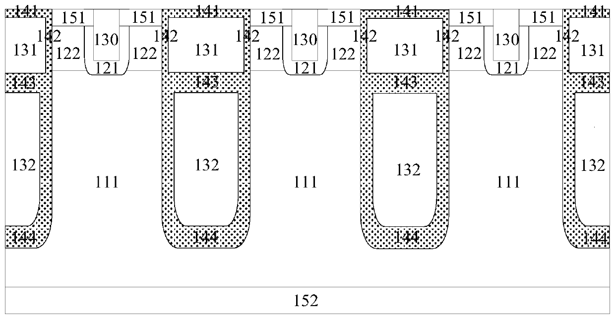
[0071] Such as Figure 5 As shown, it is a top view of the structure of the separated gate VDMOS device in Example 2. The difference between this example and the structure of Example 1 is that the connection between the shallow groove of the control gate and the deep groove of the separated gate is chamfered, which alleviates the local The curvature effect optimizes the electric field distribution and further improves the withstand voltage of the device, and its working principle is basically the same as that of Embodiment 1.


PUM


Abstract

The invention provides a separated gate VDMOS device with high channel density and a manufacturing method. The device comprises a first conductive type substrate, a first conductive type drift region,a first conductive type source electrode contact region, a second conductive type well region, a second conductive type source end contact region, a source electrode metal contact, a first dielectricoxide layer, a second dielectric oxide layer, a third dielectric oxide layer, a fourth dielectric oxide layer, a control gate polycrystalline silicon electrode and a separation gate polycrystalline silicon electrode. According to the invention, a control gate shallow groove is introduced into a device mesa region; the limitation of the existing process is met and the width of the device mesa region is not reduced; the conductive channel is added, the channel density of the device is improved, and the introduced control gate shallow groove hardly influences the withstand voltage of the device,so that the VDMOS provided by the invention has lower specific on resistance under the condition of keeping the same withstand voltage of the device, and the working loss of the device is reduced.

Description

technical field [0001] The invention belongs to the field of power semiconductors, and mainly provides a high-channel-density separated-gate VDMOS device with a three-dimensional control gate and a manufacturing method thereof. Background technique [0002] Power semiconductor devices have been widely used in consumer electronics, computers and peripherals, network communications, electronic special equipment and instruments, automotive electronics, LED Display and electronic lighting and many other aspects. Compared with conventional VDMOS devices, split gate VDMOS introduces a split gate and is short-circuited to the source, which can be regarded as an internal field version. The electric field in the drift region is modulated by MOS depletion, and higher voltage can be achieved under the same withstand voltage. Drift region concentration, lower on-resistance lower. Therefore, split-gate VDMOS has been widely used in power systems. The existing split-gate VDMOS device i...

Claims


Application Information

Patent Timeline
IPC IPC(8): H01L29/10H01L29/78H01L21/336
CPCH01L29/1033H01L29/66712H01L29/7802
Inventor 章文通何俊卿杨昆王睿乔明王卓张波李肇基
Owner UNIV OF ELECTRONIC SCI & TECH OF CHINA
Why Eureka
Try Eureka