Light-emitting apparatus and light-emitting device
A technology of light-emitting devices and light-emitting peaks, applied in the direction of electric solid-state devices, semiconductor devices, electrical components, etc., can solve the problems that LEDs cannot bear circuit wiring, unevenness, and light distribution area is too small, and achieve good light distribution characteristics and light utilization. efficiency, avoid the increase in size and cost, and simplify the effect of the connection structure
- Summary
- Abstract
- Description
- Claims
- Application Information
AI Technical Summary
Problems solved by technology
Method used
Image
Examples
Embodiment 1
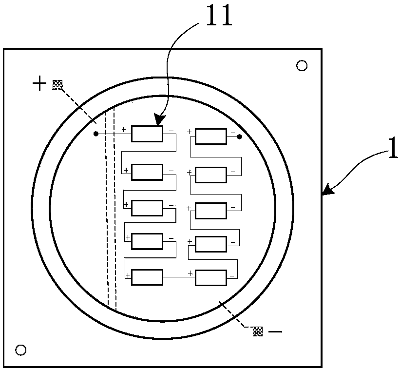
[0064] In order to solve the problems that the existing LED bracket can only protect the LED chip and lead out the positive and negative poles of the LED chip, but cannot bear the circuit wiring, this embodiment provides an LED bracket, The LED bracket provided in this embodiment has its own circuit, which can meet the requirements of connecting the LED chip to be placed in the lamp bead area on the substrate with other lamp beads (it can be other lamp beads on the same substrate, or it can be in other lamp beads) lamp beads formed on the substrate) and / or other devices on the substrate (in theory, it can be any other device, including but not limited to various chips, resistors, capacitors and other circuit devices, etc., and these devices can be set on the substrate A circuit connected to a connection point (which can be a variety of electrical connection points) that is integrated with the LED package, or not arranged on the substrate, and can be located outside the LED brac...
Embodiment 2
[0120] In order to facilitate understanding, this embodiment further exemplifies the present invention by combining several example structures of reflective lenses.
[0121] It should be understood that the reflective lens structure illustrated in this embodiment is only an example structure for illustrating the idea of the present invention, and is not limited to the following specific structures. And it should be understood that, in this embodiment, the specific size, material and combination method of the lens and the LED can be flexibly selected.
[0122]The reflective lens illustrated in this embodiment includes a lens body, a light incident surface at the bottom of the lens body, a light exit surface at the side of the lens body, and a light reflection surface at the top of the lens body. The light emitted by the LED chip of the LED is from the light incident surface. The light entering the lens body and having an included angle with the optical axis of the LED chip le...
Embodiment 3
[0144] For ease of understanding, this embodiment further exemplifies the structure of the LED used in the LED device.
[0145] This embodiment also provides an LED manufactured by using the LED bracket in the above embodiment, which includes at least one LED chip disposed in the area of the lamp bead on the substrate.
[0146] In this embodiment, the LED may also include a luminescence conversion adhesive, a lens adhesive layer or a diffusion adhesive layer disposed on the LED chip. It should be understood that the luminescence conversion adhesive in this embodiment may be a fluorescent adhesive containing phosphor powder. , can also be a colloid containing quantum dot photosensitive materials, or other luminescence conversion glue that can realize luminescence conversion, and can also include diffusion powder or silicon powder as required; in this embodiment, a luminescence conversion glue is formed on the LED chip, The method of lens adhesive layer or diffusion adhesive l...
PUM
| Property | Measurement | Unit |
|---|---|---|
| Luminescence peak wavelength | aaaaa | aaaaa |
| Luminescence peak wavelength | aaaaa | aaaaa |
| Luminescence peak wavelength | aaaaa | aaaaa |
Abstract
Description
Claims
Application Information
 - R&D
- Intellectual Property
- Life Sciences
- Materials
- Tech Scout
- Unparalleled Data Quality
- Higher Quality Content
- 60% Fewer Hallucinations
Browse by: Latest US Patents, China's latest patents, Technical Efficacy Thesaurus, Application Domain, Technology Topic, Popular Technical Reports.
© 2025 PatSnap. All rights reserved.Legal|Privacy policy|Modern Slavery Act Transparency Statement|Sitemap|About US| Contact US: help@patsnap.com


