Stealth composite material and preparation method thereof
A composite material and slurry technology, used in optics, instruments, electrical components, etc., can solve the problems of large thickness and high processing difficulty of absorbing materials, and achieve the effect of overcoming easy oxidation, solving high prices and good electrical conductivity.
- Summary
- Abstract
- Description
- Claims
- Application Information
AI Technical Summary
Problems solved by technology
Method used
Image
Examples
Embodiment 1
[0074] figure 1 It shows a schematic diagram of the structure of the composite material according to the embodiment of the present invention, from top to bottom are: infrared stealth layer 1, the first electromagnetic wave resonance control layer 2, the first wave absorbing layer 3, the second electromagnetic wave resonance control layer 4, the first Two wave-absorbing layer 5, diversion layer 6, heat insulation and infrared radiation protection layer 7.
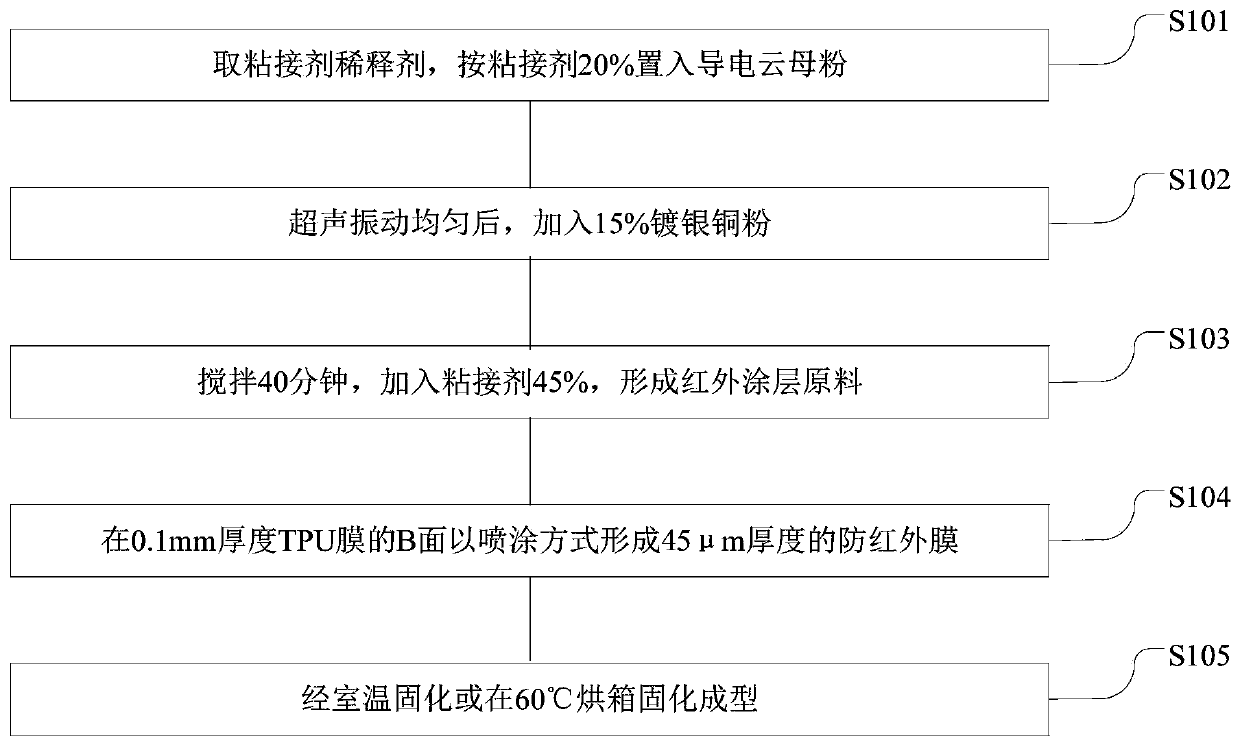
[0075] figure 2 The steps of forming the infrared stealth layer 1 according to the embodiment of the present invention are shown. The infrared stealth layer 1 is a TPU composite material with a thickness of 0.1 mm. Take 20% of the scaly conductive mica powder with a particle size of 35 μm, and 15% of the dendritic silver-plated copper powder with an average particle size of 23 μm.
[0076] S101: Put 20% of the adhesive thinner into the conductive mica powder;
[0077] S102: After uniform ultrasonic vibration, add 15% si...
Embodiment 2
[0094] Preparation of infrared stealth layer 1. For TPU composite materials, take 25% of flake-like conductive mica powder with a particle size of 40 μm, take 20% of dendritic silver-plated copper powder with an average particle size of 25 μm, and put 20% of adhesive thinner into conductive mica powder. Add silver-plated copper powder, add 35% of adhesive, and stir for 40 to 60 minutes to form an infrared stealth layer slurry; by spraying, a 50 μm thick anti-infrared film is formed on the B surface of the TPU film with a thickness of 0.3 mm; after curing at room temperature or It is cured and molded by an oven at a certain temperature.
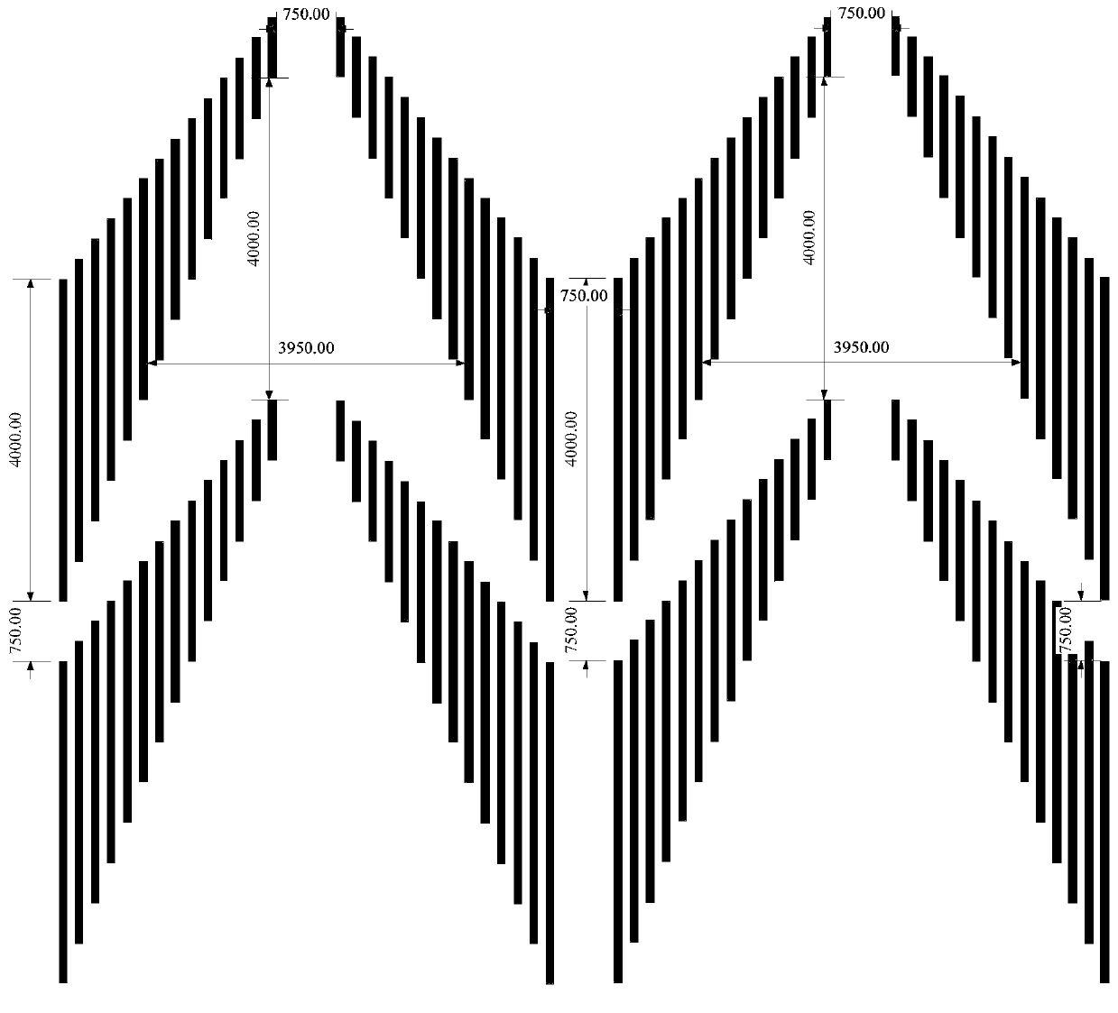
[0095] Preparation of the first electromagnetic wave resonance control layer 2 . The FPC single-sided flexible board material is selected, and the copper foil on the polyimide substrate is etched by chemical etching to form a non-equal-length line array combination. The copper foil line width is 0.15mm, the line spacing is 0.5mm, the array i...
PUM
| Property | Measurement | Unit |
|---|---|---|
| Side length | aaaaa | aaaaa |
| Thickness | aaaaa | aaaaa |
| Thickness | aaaaa | aaaaa |
Abstract
Description
Claims
Application Information
 - Generate Ideas
- Intellectual Property
- Life Sciences
- Materials
- Tech Scout
- Unparalleled Data Quality
- Higher Quality Content
- 60% Fewer Hallucinations
Browse by: Latest US Patents, China's latest patents, Technical Efficacy Thesaurus, Application Domain, Technology Topic, Popular Technical Reports.
© 2025 PatSnap. All rights reserved.Legal|Privacy policy|Modern Slavery Act Transparency Statement|Sitemap|About US| Contact US: help@patsnap.com


