Supercharge Your Innovation With Domain-Expert AI Agents!

Packaging structure and forming method thereof

A packaging structure and plastic sealing layer technology, which is applied in the manufacture of electrical components, electrical solid devices, semiconductor/solid devices, etc., can solve problems affecting the performance of the packaging structure and unstable electrical connections, etc., to improve electrical connection performance, improve accuracy, The effect of preventing loosening

Inactive Publication Date: 2019-12-03
NANTONG TONGFU MICROELECTRONICS CO LTD
View PDF7 Cites 2 Cited by
  • Summary
  • Abstract
  • Description
  • Claims
  • Application Information

AI Technical Summary

Problems solved by technology

[0004] However, in the packaging structure formed by the existing chip fan-out packaging process, the electrical connection between the wiring layer and the semiconductor chip is easily unstable, which affects the performance of the packaging structure.

Method used


Image

  • Packaging structure and forming method thereof
  • Packaging structure and forming method thereof
  • Packaging structure and forming method thereof

Examples


Embodiment Construction

[0043] As mentioned in the background art, in the packaging structure formed by the conventional chip fan-out packaging process, the electrical connection between the rewiring layer and the semiconductor chip is easily unstable, which affects the performance of the packaging structure.

[0044] Research has found that the reason why the electrical connection between the rewiring layer and the semiconductor chip in the existing fan-out packaging structure is easily unstable is that the connection position between the rewiring layer and the pad of the semiconductor chip is shifted.

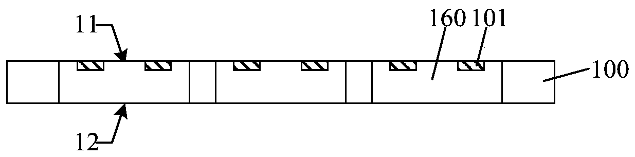
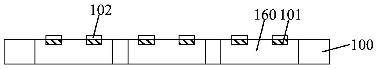
[0045] Further studies have found that the reason for the offset of the connection position between the rewiring layer and the pads of the semiconductor chip is that there are usually raised metal bumps formed on the pads of the existing semiconductor chips. , the non-functional surfaces (sides without pads) of several semiconductor chips are bonded to the carrier board by adhesive tape or adhesive l...


PUM


Abstract

The invention relates to a packaging structure and a forming method thereof. The forming method comprises the steps of: providing a plurality of semiconductor chips, wherein the functional surface ofeach semiconductor chip is provided with a bonding pad and a metal bump, the functional surface is also provided with a first plastic packaging layer, and the first plastic packaging layers cover themetal bumps; providing a carrier plate; forming a plurality of wiring layers on the surface of the carrier plate, and forming connecting pieces on the wiring layers; adhering the non-functional surfaces of the plurality of semiconductor chips to the carrier plate on one side of the connecting pieces; forming second plastic packaging layers coating the side walls of the semiconductor chips and thefirst plastic packaging layers on the non-functional surfaces on the carrier plate; performing planarizing to remove part of the first plastic packaging layers and the second plastic packaging layerson the carrier plate, and exposing the top surfaces of the metal bumps; and forming external contact structures connected with the metal bumps on the surfaces of the planarized first plastic packaginglayers and the planarized second plastic packaging layers. According to the method, the electrical connection performance of the rewiring layer and the bonding pad in the packaging structure is improved.

Description

technical field [0001] The invention relates to the field of semiconductor manufacturing, in particular to a fan-out packaging structure and a forming method thereof. Background technique [0002] Chip fan-in packaging is a manufacturing method in which rewiring and solder ball bumps are prepared on the entire wafer, and finally cut into individual chips. The final package size of this kind of package is equivalent to the chip size, which can realize the miniaturization and light weight of the package, and has a wide range of applications in portable devices. Although chip fan-in packaging can greatly reduce the packaged chip size, the number of balls on a single chip is limited, and this wafer packaging form is difficult to apply to chips with high-density I / O ports. Therefore, for chips with relatively high I / O density, if wafer-level packaging is performed, in order to ensure that the chip to be packaged and the printed circuit board can form an interconnection, the high...

Claims


Application Information

Patent Timeline
IPC IPC(8): H01L21/56H01L21/60H01L23/31
CPCH01L21/561H01L21/568H01L23/3107H01L24/02H01L24/03H01L24/11H01L24/97H01L2224/0231H01L2224/02379H01L2224/0401H01L2224/18
Inventor 石磊
Owner NANTONG TONGFU MICROELECTRONICS CO LTD
Features
  • R&D
  • Intellectual Property
  • Life Sciences
  • Materials
  • Tech Scout
  • Unparalleled Data Quality
  • Higher Quality Content
  • 60% Fewer Hallucinations
Learn More