
Gate and process method for improving filling ability of dielectric layer in zeroth layer

A technology of filling ability and process method, which is applied in the direction of circuits, electrical components, semiconductor devices, etc., can solve the problems of loss of isolation function, easy to be corroded by acid, and large trench aspect ratio, so as to reduce the formation of voids and improve filling The effect of limited ability and increased opening distance

Active Publication Date: 2022-02-01
SHANGHAI HUALI INTEGRATED CIRCUTE MFG CO LTD
View PDF3 Cites 0 Cited by
  • Summary
  • Abstract
  • Description
  • Claims
  • Application Information

AI Technical Summary

Problems solved by technology

However, as the size of the device shrinks, limited by the Design Rule, the gap between the gates becomes smaller and smaller, and the aspect ratio of the trench becomes larger, and voids will inevitably be generated during the process of filling the inner dielectric layer ( Void ), in the subsequent process, because the ILD0 at the top of the cavity is relatively thin, it is easily corroded by acid or consumed during regrinding, and an open hole is formed between the two gates, thus losing the isolation function
[0005] In order to improve the filling performance of the ILD0 layer, the ILD0 preparation process with better filling ability, such as the high aspect ratio process (HARP: High Aspect Ratio Process), is generally used. However, since this process directly uses O 2 Thermochemical reaction with TEOS (tetraethyl silicate) without plasma assistance, so voids will still form

Method used


Image

  • Gate and process method for improving filling ability of dielectric layer in zeroth layer
  • Gate and process method for improving filling ability of dielectric layer in zeroth layer
  • Gate and process method for improving filling ability of dielectric layer in zeroth layer

Examples


Embodiment Construction

[0037] In order to make the content of the present invention clearer and easier to understand, the content of the present invention will be described in detail below in conjunction with specific embodiments and accompanying drawings, but the technical content involved in the present invention is not limited to the specific embodiments given.

[0038] The present invention will be described in further detail below in conjunction with the accompanying drawings and specific embodiments. Advantages and features of the present invention will be apparent from the following description and claims. It should be noted that the drawings are all in a very simplified form and use imprecise ratios, which are only used to facilitate and clearly assist the purpose of illustrating the embodiments of the present invention.

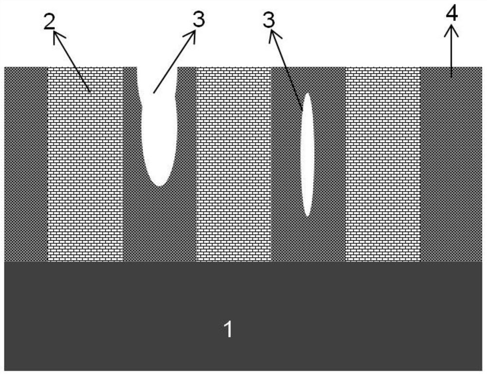
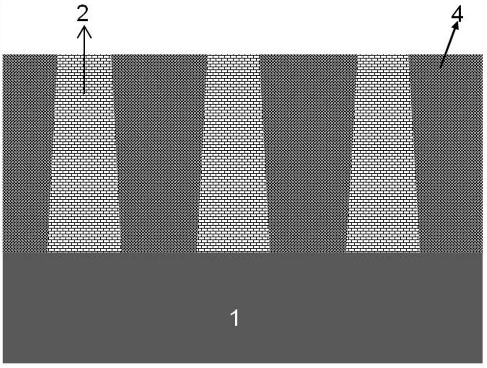
[0039] Such as figure 1 As shown, in the process node below 32nm, limited by the design rules, the gap between the gates is getting smaller and smaller, the aspect ratio ...


PUM


Abstract

The invention discloses a gate for improving the filling ability of a dielectric layer in the zeroth layer. There are a plurality of gates on a semiconductor substrate, and there is a certain distance between the plurality of gates; the cross section of the gates is as follows: Trapezoidal, i.e. the width of the top of the gate profile is smaller than the width of the bottom. The present invention replaces the traditional vertical gate design by forming a gate with a trapezoidal cross-section, thereby increasing the opening distance at the top of the trench between the gates and reducing its aspect ratio, thereby effectively improving the internal efficiency of the zeroth layer. The problem of limited filling capacity during the preparation of the dielectric layer, thereby reducing the formation of voids, improving the performance of the device and increasing the product yield. The process method described in the invention is simple and easy to implement.

Description

technical field [0001] The invention relates to the field of semiconductor device manufacturing technology, in particular to a gate that improves the filling ability of the zeroth inner dielectric layer in the gate-last process of semiconductor manufacturing. [0002] The invention also provides a process method of the gate. Background technique [0003] Complementary metal oxide semiconductor device (CMOS: Complementary Metal-Oxide-Semiconductor) manufacturing technology continues to develop along Moore's law. Increase, below 5nm, due to the tunneling effect of electrons, SiO 2 The leakage current generated as a gate dielectric is no longer acceptable. Replace SiO with high dielectric constant (high-k) dielectric 2 It can be seen that the equivalent silicon dioxide insulation thickness can be effectively reduced, and at the same time, a larger physical thickness of the gate dielectric can be obtained, thereby blocking gate leakage at the source. At present, two processe...

Claims


Application Information

Patent Timeline
Patent Type & Authority Patents(China)
IPC IPC(8): H01L21/8238H01L29/423
CPCH01L21/823828H01L21/823878H01L21/823864H01L29/42356
Inventor 刘雪娇刘哲宏许佑铨
Owner SHANGHAI HUALI INTEGRATED CIRCUTE MFG CO LTD
Features
  • Generate Ideas
  • Intellectual Property
  • Life Sciences
  • Materials
  • Tech Scout
  • Unparalleled Data Quality
  • Higher Quality Content
  • 60% Fewer Hallucinations
Learn More