An anti-interference programming method, device, equipment and storage medium

A programming method and a technology of programming pulses, which are applied in the field of semiconductors, can solve problems such as aggravating device damage and reducing device life, and achieve the effects of reducing service life, reducing misprogramming rate, and improving technical effects

Active Publication Date: 2021-04-30
GIGADEVICE SEMICON (BEIJING) INC
View PDF6 Cites 0 Cited by
  • Summary
  • Abstract
  • Description
  • Claims
  • Application Information

AI Technical Summary

Problems solved by technology

However, in the process of practical application, the level of the control gate voltage Vpass of WLn+1 or WLn-1 will also cause the transistors on the word line (WLn+1 or WLn-1) that do not want to be programmed to be programmed due to the large voltage difference. Programming, and continuous application of higher voltage on adjacent word lines will aggravate the damage of the device and reduce the life of the device

Method used


Image

  • An anti-interference programming method, device, equipment and storage medium
  • An anti-interference programming method, device, equipment and storage medium
  • An anti-interference programming method, device, equipment and storage medium

Examples


Embodiment 1

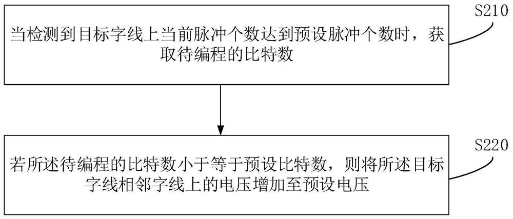
[0035] figure 2 It is a schematic flow chart of an anti-interference programming method provided by Embodiment 1 of the present invention. This embodiment is applicable to the situation of dynamically adjusting the voltage of adjacent word lines when programming a target word line. This method can be implemented by anti-interference It can be implemented by a programming device, which can be implemented in the form of software and / or hardware.

[0036] Such as figure 2 Described, the method of the present embodiment comprises:

[0037] S210, when it is detected that the number of current pulses on the target word line reaches the preset number of pulses, the number of bits to be programmed.

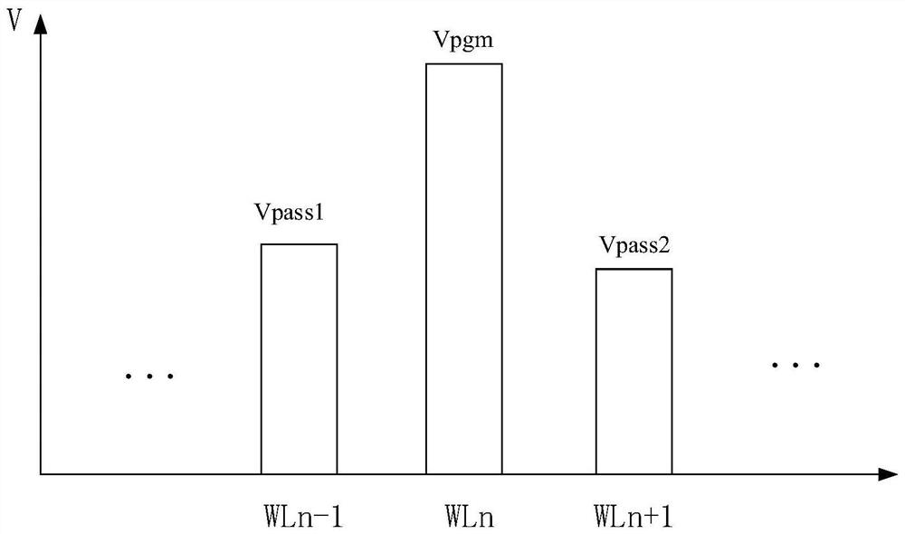
[0038] It should be noted that the erasing and writing of NAND flash memory are based on the tunneling effect. Due to the large voltage difference between the control gate and the substrate, electrons can pass through the gap between the floating gate and the silicon substrate. The i...

Embodiment 2

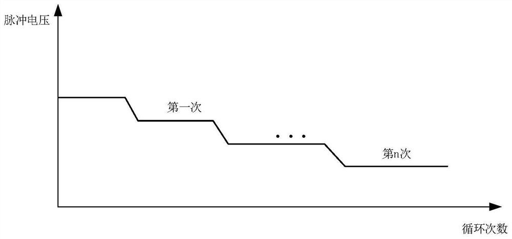
[0052] As a preferred embodiment of the above embodiment, Figure 6 It is a schematic flowchart of an anti-interference programming method provided by Embodiment 2 of the present invention, as shown in Figure 6 Described, the method of the embodiment of the present invention comprises:

[0053] S601. Obtain the current number of pulses on the target word line.

[0054] When programming the transistors on the target word line, a certain voltage and the number of pulses corresponding to the voltage need to be applied to the control gate. Exemplarily, the number of bits that need to be programmed on the target word line is 1000, and 8 pulses are required. A pulse voltage is applied to the control gate of the target word line. During the process of applying the voltage, the pulse applied to the target word line can be obtained in real time number, optionally, 1 pulse, 2 pulses, etc. are applied on the target word line.

[0055] S602. Determine whether the current number of pul...

Embodiment 3

[0065] Figure 7 It is a schematic structural diagram of an anti-jamming programming device provided by Embodiment 3 of the present invention, and the device includes: a detection module 710 and an execution module 720 . Among them, the detection module 710 is used to acquire the number of bits to be programmed when detecting that the number of current pulses on the target word line reaches the preset number of pulses; the execution module 720 is used to obtain the number of bits to be programmed if the number of bits to be programmed is less than or equal to If the number of bits is preset, the voltage on the word lines adjacent to the target word line is increased to the preset voltage.

[0066] On the basis of the above technical solution, the device also includes: a loop module, used to transfer the next pulse to As a current pulse, repeatedly performing acquiring the number of bits to be programmed until the number of bits to be programmed is less than or equal to a preset...


PUM


Abstract

The embodiment of the present invention discloses an anti-interference programming method, device, device and storage medium. The method includes: when it is detected that the number of current pulses on the target word line reaches the preset number of pulses, acquiring the number of bits to be programmed ; if the number of bits to be programmed is less than or equal to a preset number of bits, increasing the voltage on a word line adjacent to the target word line to a preset voltage. The technical solution of the embodiment of the present invention not only reduces the misprogramming rate of the target word line and adjacent word line transistors, the interference of the voltage of the adjacent word line to the array, and the device damage, and also improve the technical effect of device service life.

Description

technical field [0001] Embodiments of the present invention relate to the field of semiconductor technology, and in particular, to an anti-interference programming method, device, equipment, and storage medium. Background technique [0002] The memory cell of flash memory is a three-terminal device and has the same names as a field effect transistor: source, drain, and gate. The difference between flash memory and FET is that there is a floating gate in flash memory, which is set between the control gate and the substrate; there is a silicon dioxide insulating layer between the control gate and the silicon substrate to protect the floating gate. The charge in the gate will not leak. Due to the structural characteristics of the flash memory, the storage unit of the flash memory has a certain charge retention capability. Flash memory is also a voltage-controlled device. The flash memory that is often used at this stage is NAND flash memory. Among them, the erasing and writin...

Claims


Application Information

Patent Timeline
Patent Type & Authority Patents(China)
IPC IPC(8): G11C16/34G11C16/08G11C16/04
CPCG11C16/0408G11C16/08G11C16/3422G11C16/3427
Inventor 刘会娟陈立刚张科科
Owner GIGADEVICE SEMICON (BEIJING) INC
Why Eureka
Try Eureka