Supercharge Your Innovation With Domain-Expert AI Agents!

Display panel and preparation method thereof

A technology for display panels and preparation steps, which is applied in semiconductor/solid-state device manufacturing, electrical components, electric solid-state devices, etc. It can solve problems such as poor flexibility, affecting the optical performance of display panels, and poor water and oxygen resistance performance, so as to reduce fracture risk, improve the ability to isolate water and oxygen, and improve the effect of adhesion

Active Publication Date: 2019-12-13
WUHAN CHINA STAR OPTOELECTRONICS SEMICON DISPLAY TECH CO LTD
View PDF6 Cites 5 Cited by
  • Summary
  • Abstract
  • Description
  • Claims
  • Application Information

AI Technical Summary

Problems solved by technology

[0007] The invention provides a display panel and its preparation method to solve the technical problems existing in the prior art of poor water and oxygen barrier performance, poor flexibility and affecting the optical performance of the display panel

Method used


Image

  • Display panel and preparation method thereof
  • Display panel and preparation method thereof
  • Display panel and preparation method thereof

Examples


Embodiment 1

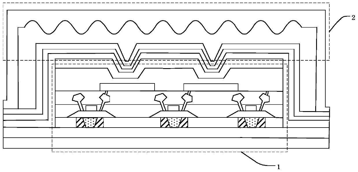
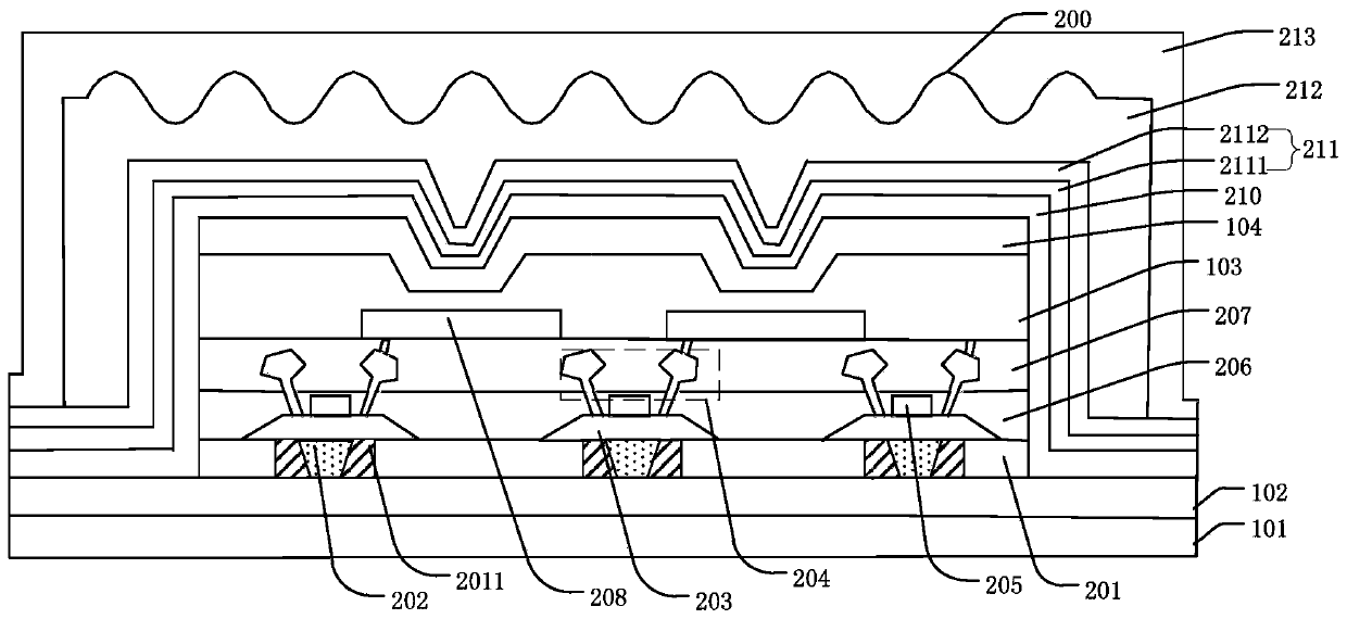
[0034] Such as figure 1 As shown, this embodiment provides a display panel, including a base substrate 1 and a thin film encapsulation layer 2 , and the thin film encapsulation layer 2 is the upper surface of the base substrate 1 .

[0035] Such as figure 2 As shown, the base substrate 1 includes a glass substrate 101 , a PI substrate 102 , a thin film transistor, a pixel definition layer 103 and a light emitting layer 104 .

[0036] The glass substrate 101 is a glass substrate in the prior art. The PI substrate 102 is a flexible substrate, and its material is mainly polyimide (PI). The PI material can effectively improve light transmittance. Each thin film transistor includes an active layer 201 (P-type doped), a polysilicon layer 202 , a dielectric layer 203 , source and drain electrodes 204 , a gate electrode 205 , an insulating layer 206 , a planar layer 207 and an anode 208 . Specifically, a doped region 2011 is provided in the active layer 201, and the doped region 2...

Embodiment 2

[0062] Such as Figure 7 As shown, this embodiment provides a display panel, which includes most of the technical features of the display panel described in Embodiment 1, and its distinguishing feature is that in Embodiment 2, the laminated film layer 211 is provided on the second inorganic layer 210 and the organic between the first inorganic layer 210 and the organic layer 212 instead of between the first inorganic layer 210 and the organic layer 212 .

[0063] Such as Figure 7 As shown, the thin film encapsulation layer in the display panel includes a first inorganic layer 210 , an organic layer 212 , a stacked film layer 211 and a second inorganic layer 213 from bottom to top.

[0064] Each stacked film layer 211 includes a dense film layer 2111 and an interlayer 2112 .

[0065] In this embodiment, the transition layer 2112 is disposed on the upper surface of the organic layer 212 , and the dense film layer 2111 is disposed on the upper surface of the transition layer 2...


PUM

PropertyMeasurementUnit
thicknessaaaaaaaaaa
thicknessaaaaaaaaaa
thicknessaaaaaaaaaa

Abstract

The invention provides a display panel and a preparation method thereof. The display panel comprises a substrate and a thin film packaging layer, wherein the thin film packaging layer comprises a first inorganic layer, an organic layer and a laminated film layer. The preparation method for the display panel comprises a substrate providing step and a thin film packaging layer preparing step. The thin film packaging layer preparing step comprises a first inorganic layer packaging substep, a laminated film layer packaging substep, an organic layer packaging substep and a second inorganic layer packaging substep. The invention provides a display panel and a preparation method thereof. The patterned surface is arranged on the surface of the organic layer, so that the stress release capability of the film layer of the patterned surface is improved, the risk that the thin film packaging layer is broken in the bending process of the display panel is reduced, and the reliability of the thin film packaging layer and the optical performance of the display panel are improved.

Description

technical field [0001] The invention relates to the display field, in particular to a display panel and a preparation method thereof. Background technique [0002] Compared with the traditional LCD, the display panel has the advantages of light weight, wide viewing angle, fast response time, low temperature resistance, and high luminous efficiency. Therefore, it has been regarded as the next generation of new display technology in the display industry, especially OLED can be made into a flexible device that can be bent on a flexible substrate, which is a huge advantage unique to OLED. In order to realize the advantages of OLED (flexible display), thin film encapsulation (TFE) technology is an essential core technology. [0003] The deadly killer of the display panel is the water and oxygen existing in the external environment. The intrusion of water and oxygen from the outside can be divided into two categories: the first is that water and oxygen directly penetrate the TFE...

Claims


Application Information

Patent Timeline
Patent Type & Authority Applications(China)
IPC IPC(8): H01L51/52H01L51/56
CPCH10K59/12H10K59/8731H10K50/844H10K71/00
Inventor 郭天福
Owner WUHAN CHINA STAR OPTOELECTRONICS SEMICON DISPLAY TECH CO LTD
Features
  • R&D
  • Intellectual Property
  • Life Sciences
  • Materials
  • Tech Scout
  • Unparalleled Data Quality
  • Higher Quality Content
  • 60% Fewer Hallucinations
Learn More