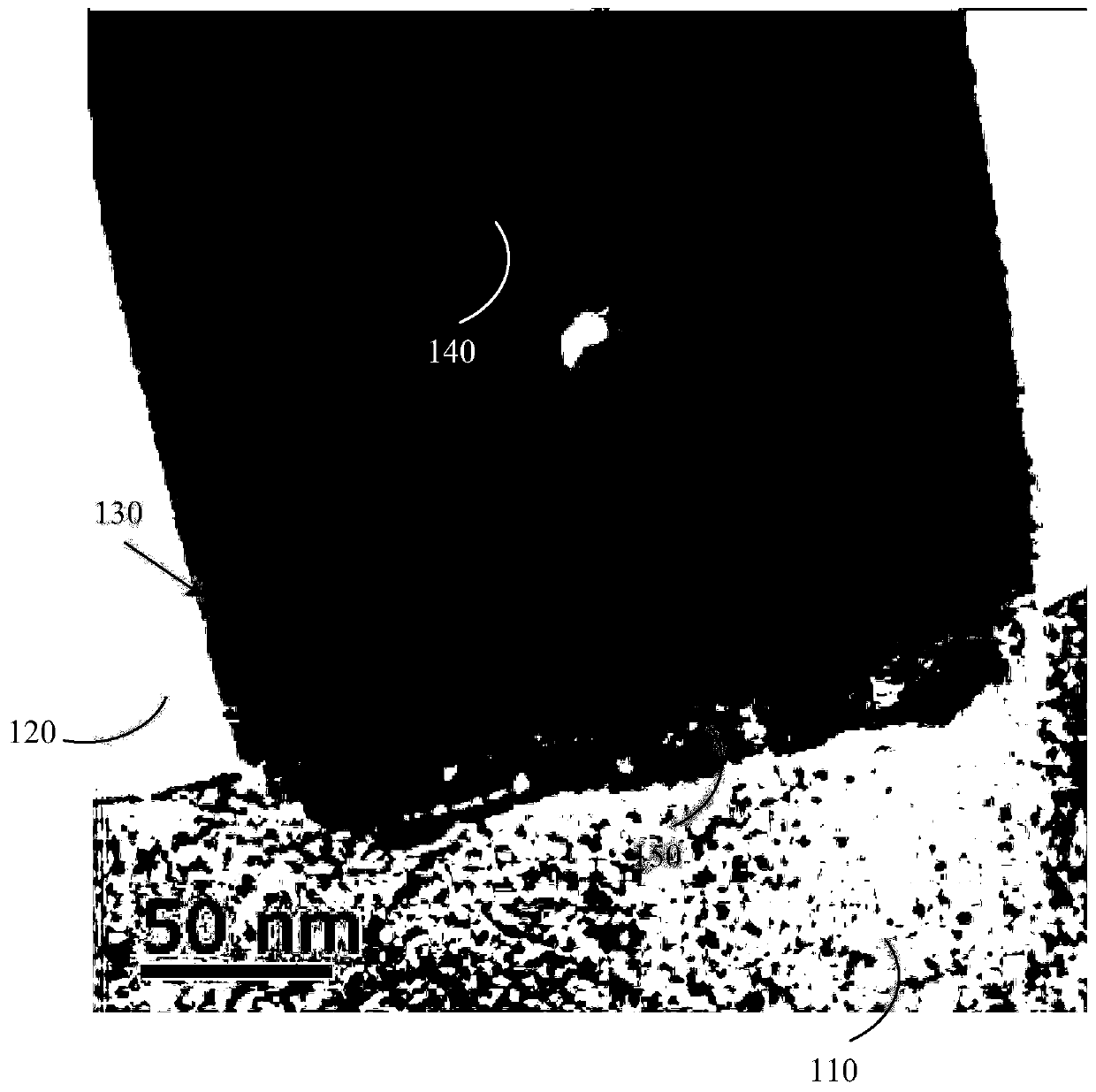
Characterization method for metal silicide
A metal silicide and characterization technology, applied in the field of metal silicide characterization, can solve problems such as time-consuming, complicated operation, complicated operation process and result analysis, and achieve the effect of improving image contrast
- Summary
- Abstract
- Description
- Claims
- Application Information
AI Technical Summary
Problems solved by technology
Method used
Image

Examples
Embodiment Construction
[0026] In order to make the above-mentioned objects, features and advantages of the present invention more obvious and understandable, the specific embodiments of the present invention will be described in detail below with reference to the accompanying drawings.
[0027] In the following description, many specific details are set forth in order to fully understand the present invention, but the present invention can also be implemented in other ways different from those described here, so the present invention is not limited by the specific embodiments disclosed below.
[0028] As shown in the present application and claims, unless the context clearly indicates exceptions, the words "a", "an", "an" and / or "the" do not specifically refer to the singular, but may also include the plural. Generally speaking, the terms "include" and "include" only suggest that the clearly identified steps and elements are included, and these steps and elements do not constitute an exclusive list, and t...
PUM
 Abstract
Description
Claims
Application Information
 - R&D
- Intellectual Property
- Life Sciences
- Materials
- Tech Scout
- Unparalleled Data Quality
- Higher Quality Content
- 60% Fewer Hallucinations
Browse by: Latest US Patents, China's latest patents, Technical Efficacy Thesaurus, Application Domain, Technology Topic, Popular Technical Reports.
© 2025 PatSnap. All rights reserved.Legal|Privacy policy|Modern Slavery Act Transparency Statement|Sitemap|About US| Contact US: help@patsnap.com