Polycrystalline silicon thin film manufacturing method

A polysilicon thin film and a production method technology, which are applied in the manufacture of semiconductor/solid state devices, electrical components, circuits, etc., can solve the problems affecting the film formation quality of polysilicon thin films, such as electrical reliability, small grain size, and high process cost.

Active Publication Date: 2019-12-17
EVERDISPLAY OPTRONICS (SHANGHAI) CO LTD
View PDF7 Cites 0 Cited by
  • Summary
  • Abstract
  • Description
  • Claims
  • Application Information

AI Technical Summary

Problems solved by technology

[0003] At present, when preparing polysilicon thin films, a layer of amorphous silicon thin film is generally deposited on a glass substrate first, and then the amorphous silicon thin film is converted into a polysilicon thin film by laser laser technology. When the process temperature required by the deposition process is high, and The temperature resistance of glass subst

Method used


Image

  • Polycrystalline silicon thin film manufacturing method
  • Polycrystalline silicon thin film manufacturing method
  • Polycrystalline silicon thin film manufacturing method

Examples


Embodiment Construction

[0035] The present invention will be further described in detail below in conjunction with the accompanying drawings and embodiments. It should be understood that the specific embodiments described here are only used to explain the present invention, but not to limit the present invention. In addition, it should be noted that, for the convenience of description, only some structures related to the present invention are shown in the drawings but not all structures. Throughout this specification, the same or similar reference numerals represent the same or similar structures, elements or processes. It should be noted that, in the case of no conflict, the embodiments in the present application and the features in the embodiments can be combined with each other.

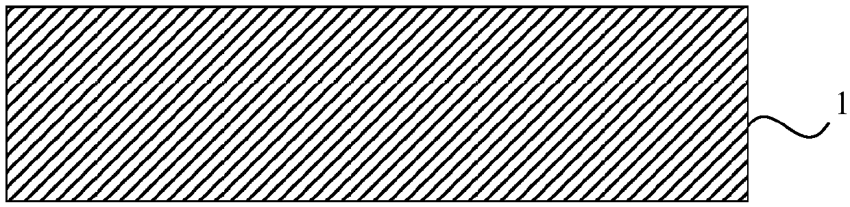
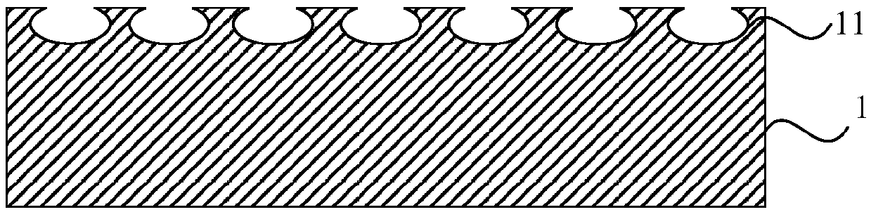
[0036] An embodiment of the present invention provides a polysilicon thin film manufacturing method. The polysilicon thin film manufacturing method includes providing a first substrate and setting the temperature resist...


PUM


Abstract

An embodiment of the invention discloses a polycrystalline silicon thin film manufacturing method. The polycrystalline silicon thin film manufacturing method comprises the steps: providing a first substrate, wherein the temperature resistance temperature of the first substrate is larger than or equal to 600 DEG C; forming a polycrystalline silicon thin film on the first substrate; and transferringthe formed polycrystalline silicon thin film to a glass substrate. According to the technical scheme provided by the invention, by forming the polycrystalline silicon thin film on the first substratewith higher temperature resistance, and then, transferring the formed polycrystalline silicon thin film onto the glass substrate, the problem that the manufacturing process of the polycrystalline silicon thin film is limited due to the temperature resistance of the glass substrate is avoided; and compared with a laser process adopted in the prior art, the method can allow crystal grains of the polycrystalline silicon thin film to reach a larger size, wherein crystal boundary defects of the polycrystalline silicon thin film with larger crystal grain size are fewer, so that the film forming quality of the formed polycrystalline silicon thin film and the electrical reliability of the polycrystalline silicon thin film are improved.

Description

technical field [0001] The embodiments of the present invention relate to the technical field of semiconductor manufacturing, and in particular to a method for manufacturing a polysilicon thin film. Background technique [0002] Low-temperature polysilicon has the advantages of regular atomic arrangement and high carrier mobility. In the field of liquid crystal display, low-temperature polysilicon has a high driving current, which can speed up the response time of liquid crystal, reduce the volume of thin-film transistors, and increase the light-transmitting area, making liquid crystal display The brightness and resolution of the panel are high, so low-temperature polysilicon is widely used in the manufacturing process of the thin film transistor to prepare the active layer. [0003] At present, when preparing polysilicon thin films, a layer of amorphous silicon thin film is generally deposited on a glass substrate first, and then the amorphous silicon thin film is converted...

Claims


Application Information

Patent Timeline
IPC IPC(8): H01L21/02H01L21/78
CPCH01L21/02532H01L21/02595H01L21/7806
Inventor 曾煌
Owner EVERDISPLAY OPTRONICS (SHANGHAI) CO LTD
Why Eureka
Try Eureka