Cutting process for large-size silicon wafer
A cutting process and technology of silicon wafers, applied in the direction of work accessories, manufacturing tools, stone processing equipment, etc., can solve problems such as poor warpage consistency, easy bending of the surface, and excessive silicon powder
- Summary
- Abstract
- Description
- Claims
- Application Information
AI Technical Summary
Problems solved by technology
Method used
Image

Examples
Embodiment Construction
[0024] The present invention will be described in detail below in conjunction with the accompanying drawings and specific embodiments.
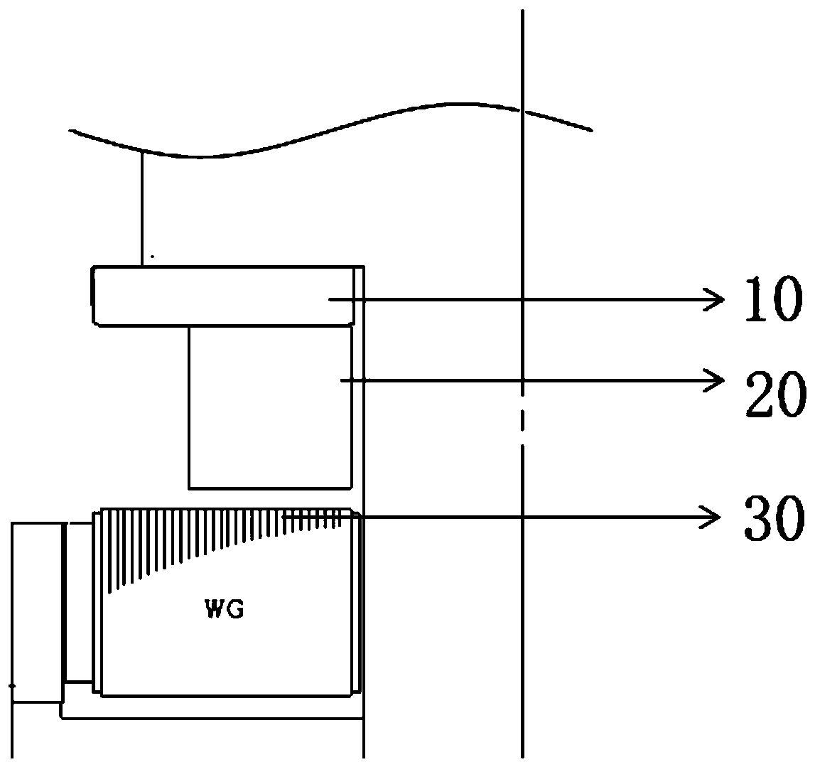
[0025] The present invention proposes a large-size silicon wafer cutting process, such as figure 1 As shown, the steps include:
[0026] S1: bonding the silicon round rod 20 to the resin plate.
[0027] Before sticking the rod, the silicon round rod 20 with a length of 350 mm and a diameter of 300 mm is cleaned with absolute ethanol on the outer edge wall surface of the silicon round rod 20 in the length direction to remove surface impurities, which is convenient for sticking the rod in the next step. Then the silicon round rod 20 after wiping is placed on the automatic sticking stick orientation instrument, the crystal orientation of the silicon round stick 20 is tested and the sticking operation is carried out. The sticking stick orientation instrument model is DX-7DZ. Q-Bond series stick glue is used in the sticking process. The glue use...
PUM
| Property | Measurement | Unit |
|---|---|---|
| diameter | aaaaa | aaaaa |
| diameter | aaaaa | aaaaa |
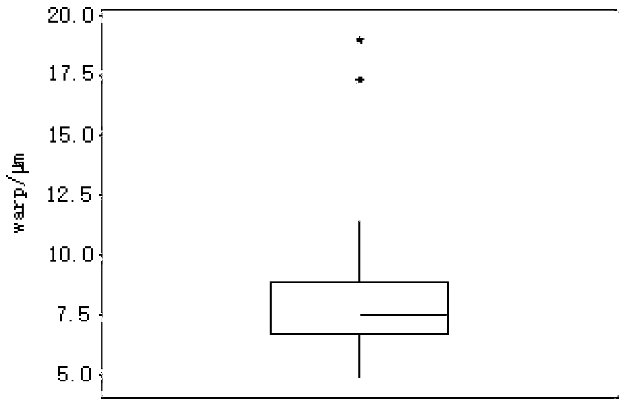
| warpage | aaaaa | aaaaa |
Abstract
Description
Claims
Application Information
 - R&D
- Intellectual Property
- Life Sciences
- Materials
- Tech Scout
- Unparalleled Data Quality
- Higher Quality Content
- 60% Fewer Hallucinations
Browse by: Latest US Patents, China's latest patents, Technical Efficacy Thesaurus, Application Domain, Technology Topic, Popular Technical Reports.
© 2025 PatSnap. All rights reserved.Legal|Privacy policy|Modern Slavery Act Transparency Statement|Sitemap|About US| Contact US: help@patsnap.com