Semiconductor device forming method

A semiconductor and device technology, applied in the field of semiconductor device formation, can solve problems such as poor electrical performance

Active Publication Date: 2018-01-16
SEMICON MFG INT (SHANGHAI) CORP +1
View PDF4 Cites 3 Cited by
  • Summary
  • Abstract
  • Description
  • Claims
  • Application Information

AI Technical Summary

Problems solved by technology

[0005] However, the semiconductor devices formed by the pri

Method used


Image

  • Semiconductor device forming method
  • Semiconductor device forming method
  • Semiconductor device forming method

Examples


Embodiment Construction

[0032] According to the background art, the electrical performance of semiconductor devices formed in the prior art is relatively poor.

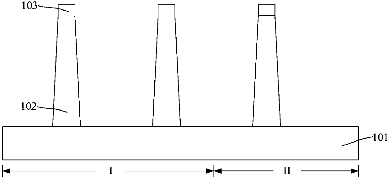
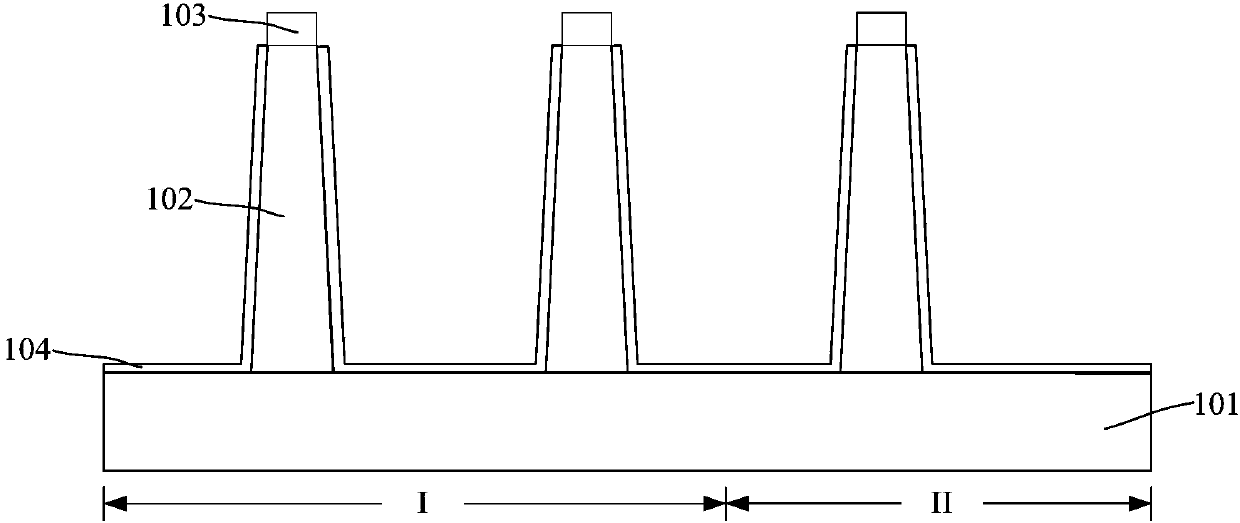
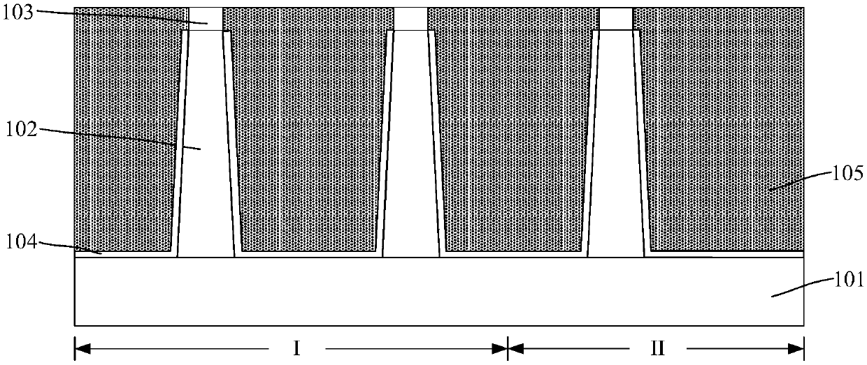
[0033] It is found through research that due to the different operating voltages of the core device and the input-output device, the thickness of the gate dielectric layer of the core device and the input-output device is different. The gate dielectric layer includes an oxide layer and a high-k gate dielectric layer on the surface of the oxide layer. The thickness of the oxide layer in the core device is smaller than the thickness of the oxide layer in the input-output device, so that the thickness of the gate dielectric layer of the core device and the input-output device is different. Usually, the thicker peripheral oxide layer of the input and output devices is formed first, and then the thinner core oxide layer of the core device is formed.

[0034] The process steps of forming the peripheral oxide layer and the core oxide layer include:...


PUM

PropertyMeasurementUnit
Thicknessaaaaaaaaaa

Abstract

The invention discloses a semiconductor device forming method. The method comprises steps that: a base comprising a first area and a second area is provided, wherein the first area base and the secondarea base are provided with first oxidation layers; an etching process is carried out to etch and remove the first oxidation layer with a first thickness in the first area; after the etching processis carried out, the remaining first oxidation layer in the first area is subjected to a cleaning process; the etching process and the cleaning process are carried out alternatively until the first oxidation layer in the first area is removed; and a second oxidation layer is formed on the first area base, wherein the thickness of the second oxidation layer is different from that of the first oxidation layer. The first area base can be prevented from being etched and damaged, the first area base can thus keep a good surface morphology, and the electrical performance of the formed semiconductor device is improved.

Description

technical field [0001] The invention relates to the technical field of semiconductor manufacturing, in particular to a method for forming a semiconductor device. Background technique [0002] A Metal-Oxide-Semiconductor (MOS, Metal-Oxide-Semiconductor) device has been known as one of the commonly used semiconductor devices in integrated circuits. The MOS device includes: P-type metal oxide semiconductor (PMOS, P-type MOS) device, N-type metal oxide semiconductor (NMOS, N-type MOS) device and complementary metal oxide semiconductor (CMOS, Complementary MOS) device. [0003] Metal oxide semiconductor devices are mainly divided into core (Core) devices and input and output (IO, Input and Output) devices according to their functions. According to the electrical types of metal oxide semiconductor devices, core devices can be divided into core NMOS devices and core PMOS devices, and input-output devices can be divided into input-output NMOS devices and input-output PMOS devices....

Claims


Application Information

Patent Timeline
IPC IPC(8): H01L21/8234H01L27/088
Inventor 李勇
Owner SEMICON MFG INT (SHANGHAI) CORP
Why Eureka
Try Eureka