A method for cutting wafers on three sides

A cutting method and wafer technology, applied in the manufacturing of electrical components, circuits, semiconductor/solid-state devices, etc., can solve problems such as increasing the difficulty of operation, affecting production capacity, and reducing the reliability of subsequent processes.

Active Publication Date: 2021-03-16
JIANGSU UNION SEMICON
View PDF6 Cites 0 Cited by
  • Summary
  • Abstract
  • Description
  • Claims
  • Application Information

AI Technical Summary

Problems solved by technology

[0003] The wafer cutting process in the prior art is to separate multiple ICs from the wafer. One grain formed after cutting is one IC. The cutting in the first direction is completed through the STEP double-knife synchronous cutting mode, and the table is processed. After rotating 90 degrees, the cutting action in the second direction perpendicular to the first direction is completed; the disadvantage is that: after the double-knife synchronous cutting in the first direction, the double-knife synchronous cutting process in the second direction is carried out. The viscosity of the adhesive film decreases, and the simultaneous cutting of the wafer by two knives will increase the vibration amplitude, resulting in cracks on the back of the IC. The cracks on the back of the IC cannot be inspected by the inspection machine. To ensure product quality, the operator needs to manually check the IC. Turning over the back for inspection increases the difficulty of the operation in the manufacturing process, affects the production capacity, and reduces the reliability of the subsequent process. It is easy to cause IC breakage and abnormal pressing at the client end, resulting in customer complaints

Method used


Image

  • A method for cutting wafers on three sides
  • A method for cutting wafers on three sides
  • A method for cutting wafers on three sides

Examples


Embodiment Construction

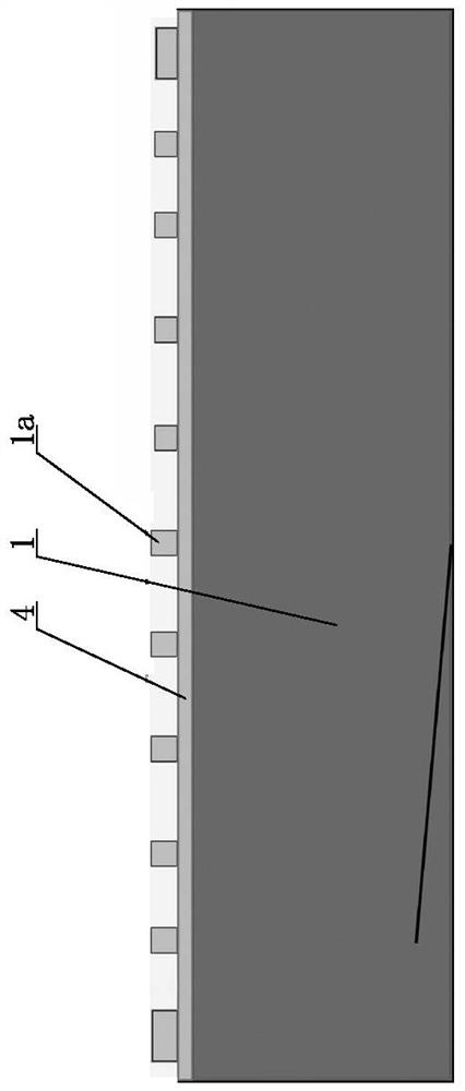
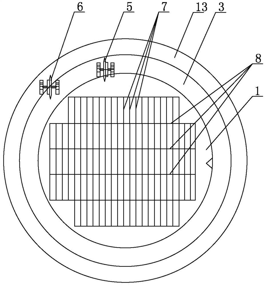
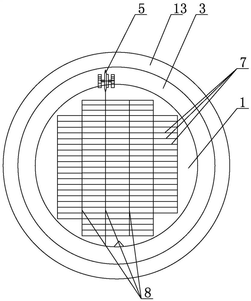
[0034] like Figure 2-11 As shown, it is a three-side cutting method of a wafer, including the following steps:

[0035] (1) Provide a wafer 1, the diameter of the wafer 1 is 203 or 305 mm; the surface of the wafer 1 is provided with gold bumps 1a; the wafer 1 is fixed on the adhesive film layer 3 through the adhesive layer 2 , the surface area of ​​the adhesive film layer 3 is greater than the surface area of ​​the wafer 1, the center of the wafer 1 and the adhesive film layer 3 overlaps, the outer peripheral edge of the adhesive film layer 3 is fixed with an outer frame, and the surface of the wafer 1 is covered with a passivation protection layer 4;

[0036] (2) The wafer 1 is transported to the rotatable wafer 1 stage located under the cutting mechanism. The wafer 1 is placed horizontally. The wafer 1 is set corresponding to the cutting mechanism. The cutting mechanism includes a laterally movable knife seat 1 and Knife seat two, there is a transverse distance between kn...


PUM


Abstract

The invention discloses a wafer three-sided cutting method in the technical field of semiconductors. The method includes the following steps: providing a wafer, conveying the wafer to a rotatable wafer stage below a cutting mechanism, enabling a detection camera to perform scanning and analyzing to form a plurality of horizontal cutting channels and longitudinal cutting channels arranged at intervals, and enabling first and second cutters to cut the wafer along corresponding longitudinal cutting channels; rotating the wafer stage by 90 degrees, enabling the first cutter to cut the wafer alongthe respective horizontal cutting channels, and enabling the first cutter to cut out a groove on the wafer along the horizontal cutting channels; enabling the second cutter to the wafer along the respective horizontal cutting channels, and enabling the second cutter to through cut the wafer along the horizontal cutting channels so as to separate an IC. The method can separate the IC from the waferin three cutting steps, can reduce a risk of cracks on the back of the IC, enhances the reliability of the IC, reduce product stress concentration, and improves the quality of the cut IC product.

Description

technical field [0001] The invention belongs to the technical field of semiconductors, and in particular relates to a three-side cutting method of a wafer. Background technique [0002] At present, with the rapid development of the optoelectronic industry, the demand for highly integrated and high-performance semiconductor wafers is also increasing. In order to greatly save costs and improve manufacturing efficiency, integrated circuit chips are often deposited on wafers in mass production. Or circuit element structure, and then divided into individual dies, and finally packaged and soldered, therefore, the wafer cutting process has an important impact on improving yield and packaging efficiency. [0003] The wafer cutting process in the prior art is to separate multiple ICs from the wafer. One grain formed after cutting is one IC. The cutting in the first direction is completed through the STEP double-knife synchronous cutting mode, and the table is processed. After rotati...

Claims


Application Information

Patent Timeline
Patent Type & Authority Patents(China)
IPC IPC(8): H01L21/304H01L21/67
CPCH01L21/304H01L21/67253
Inventor 陈志远姜红涛高美山刘磊黄金良
Owner JIANGSU UNION SEMICON
Why Eureka
Try Eureka