Method for processing thin substrate
A processing method and substrate technology, which are applied in the manufacture of electrical components, electric solid-state devices, and semiconductor/solid-state devices, etc., can solve the problems of fragile manufacturing equipment, difficult for detectors to correctly recognize the substrate, and equipment unable to correctly recognize the substrate, etc. Achieve the effect of reducing process limitations and ensuring machining accuracy
- Summary
- Abstract
- Description
- Claims
- Application Information
AI Technical Summary
Problems solved by technology
Method used
Image

Examples
Embodiment 1
[0031] Embodiment 1 of the present application provides a method for processing a thin substrate. The method of this embodiment may include the following steps:
[0032] Step 101, forming a plurality of recesses on the second main surface of the supporting substrate;
[0033] Step 102, bonding the first main surface of the sheet substrate to the first main surface of the supporting substrate;
[0034] Step 103, performing microfabrication on the second main surface of the sheet substrate;
[0035] Step 104 , removing the supporting substrate from the sheet substrate.
[0036] In this embodiment, the first main surface of the support substrate is located behind the second main surface of the support substrate, and the first main surface of the sheet substrate is located behind the second main surface of the sheet substrate.
[0037] According to the processing method of the sheet substrate of this embodiment, since a plurality of recesses are formed on the back surface of th...
example 1
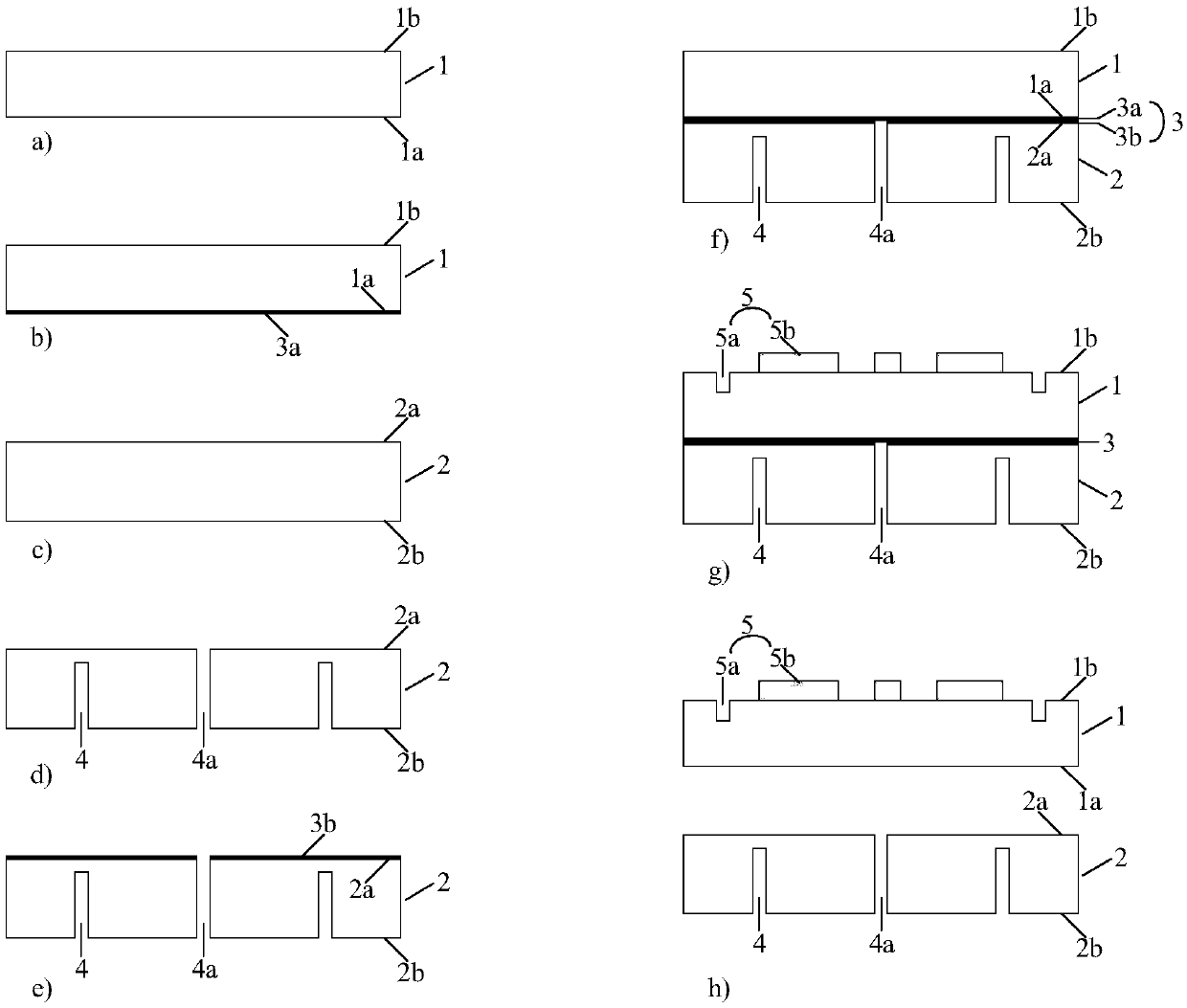
[0061] figure 1 It is a schematic diagram of an example of the processing method of the sheet substrate of this embodiment. Below, combine figure 1 , the processing method of the thin substrate of this example will be described in detail.
[0062] Such as figure 1 As shown in a), the semiconductor substrate 1 is first prepared, and the semiconductor substrate 1 is the thin substrate of this embodiment. Here, the semiconductor substrate refers to a thin substrate suitable for processing in a semiconductor manufacturing process, and does not mean that the Thin substrates can only be made of semiconductor materials.
[0063] In this embodiment, the semiconductor substrate 1 has two corresponding main surfaces, namely a first main surface 1a and a second main surface 1b. The semiconductor substrate 1 may be a wafer commonly used in the semiconductor manufacturing field, such as a silicon wafer, a silicon on insulator (SOI: Silicon On Insulator) wafer, a silicon germanium wafer...
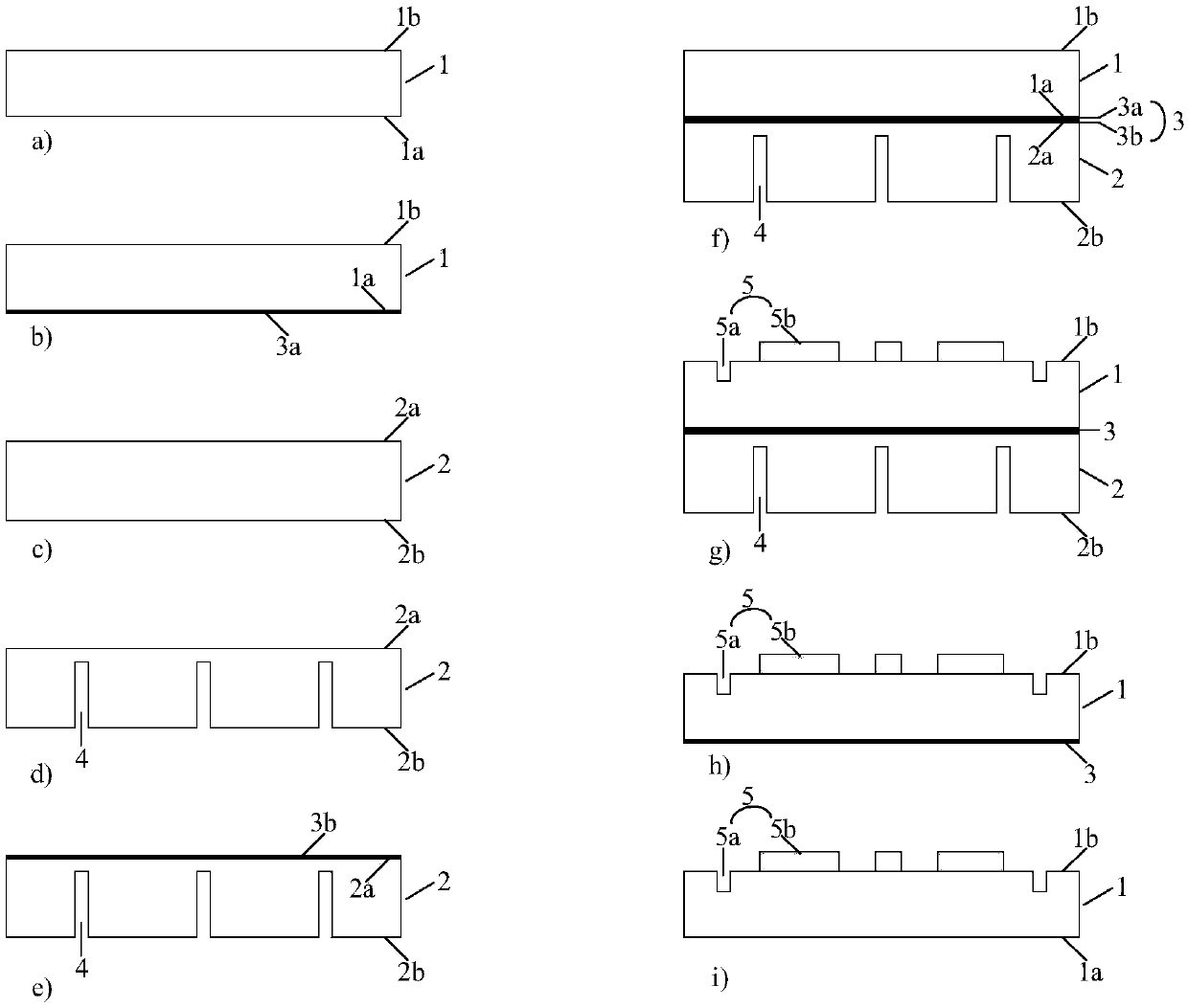
example 2
[0073] figure 2 It is a schematic diagram of another example of the processing method of the sheet substrate of this embodiment. Below, combine figure 2 , the processing method of the thin substrate of the present example 2 will be described in detail. Parts similar to Example 1 in this Example 2 will not be described in detail.
[0074] Such as figure 2 As shown in a), firstly, the semiconductor substrate 1 is prepared. In this embodiment, the semiconductor substrate 1 has two corresponding main surfaces, namely a first main surface 1a and a second main surface 1b. The semiconductor substrate 1 can be the same as that of the first embodiment. As a special example, the semiconductor substrate 1 is a quartz substrate with a thickness of 250 microns and a diameter of 200 mm.
[0075] next step, such as figure 2 As shown in b), an inorganic thin film 3 a is formed on the first main surface 1 a of the semiconductor substrate 1 . The inorganic thin film 3a can be formed...
PUM
| Property | Measurement | Unit |
|---|---|---|
| Thickness | aaaaa | aaaaa |
| Diameter | aaaaa | aaaaa |
| Thickness | aaaaa | aaaaa |
Abstract
Description
Claims
Application Information
PatSnap Eureka turns technology decisions into work you can execute. Powered by our Innovation Knowledge Graph, it runs expert workflows across engineering, life sciences, materials and intellectual property. Get your review-ready output in minutes.


