Micro-light emitting diode display and manufacturing method thereof

A technology of micro-light-emitting diodes and manufacturing methods, applied in the direction of electric solid-state devices, semiconductor devices, electrical components, etc., can solve problems such as low reliability, complicated manufacturing process, and complicated structure of the transfer head, and achieve quality improvement, simple manufacturing process, and simple structure Effect

Pending Publication Date: 2019-12-20
SHENZHEN KECHUANG DIGITAL DISPLAY TECH
View PDF0 Cites 1 Cited by
  • Summary
  • Abstract
  • Description
  • Claims
  • Application Information

AI Technical Summary

Problems solved by technology

The above-mentioned methods are complex in manufacturing process, relatively complex in structure of the transfer head, low in reliability, and require additional manufacturing costs

Method used


Image

  • Micro-light emitting diode display and manufacturing method thereof
  • Micro-light emitting diode display and manufacturing method thereof
  • Micro-light emitting diode display and manufacturing method thereof

Examples


Embodiment Construction

[0045] In order to further illustrate the technical means adopted by the present invention and its effects, the following describes in detail in conjunction with preferred embodiments of the present invention and accompanying drawings.

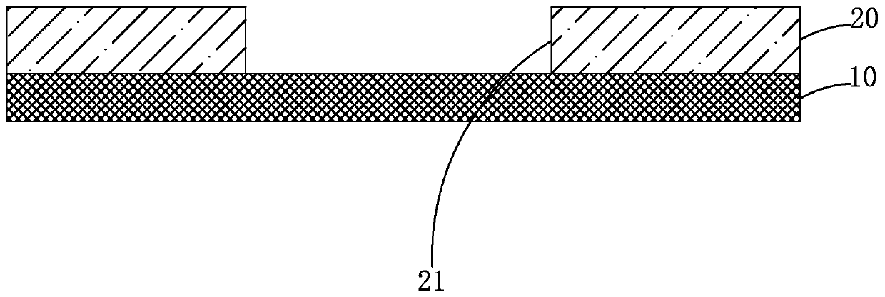
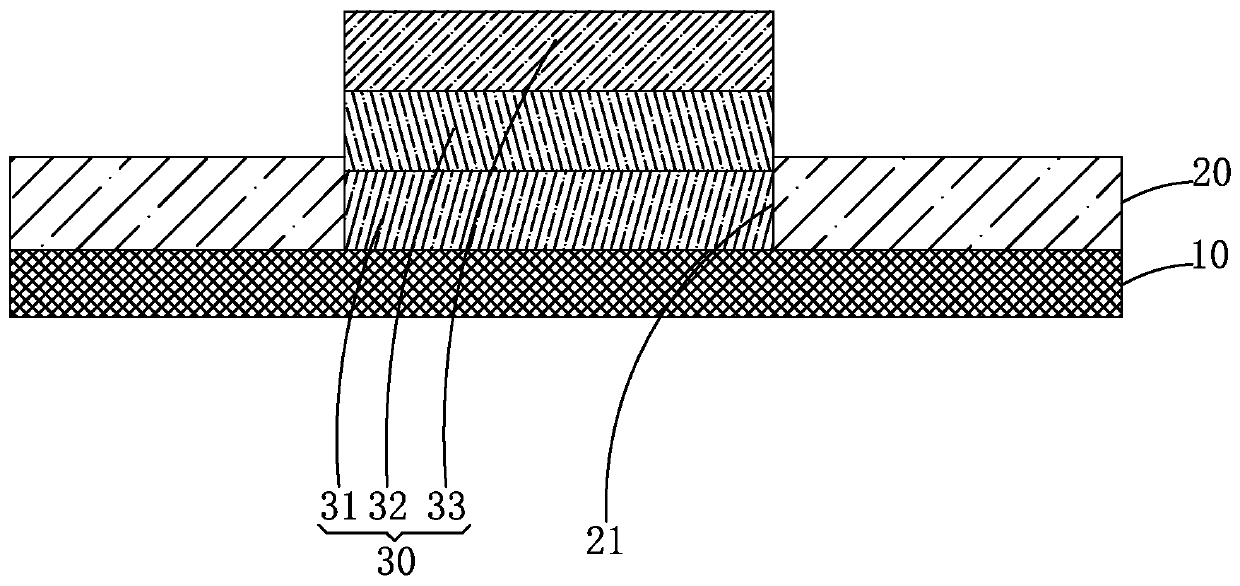
[0046] see Figure 1 to Figure 9 , the present invention provides a kind of manufacturing method of micro light-emitting diode display, comprises the following steps:

[0047] Step S1, please refer to figure 2, providing a growth substrate 10 . A first insulating layer 20 is formed on the growth substrate 10 , and the first insulating layer 20 is patterned to form openings 21 .

[0048] Specifically, the material of the growth substrate 10 is sapphire, silicon or silicon carbide.

[0049] Specifically, in the step S1, the first insulating layer 20 is formed on the growth substrate 10 by atomic layer deposition (ALD) or plasma enhanced chemical vapor deposition (CVD).

[0050] Specifically, in the step S1, the opening 21 is formed by patte...


PUM


Abstract

The invention provides a micro-light emitting diode display and a manufacturing method thereof. The manufacturing method of the micro-light emitting diode display comprises the steps of forming a first insulating layer with an opening on a growth substrate and forming a micro-light emitting diode function layer in the opening on the growth substrate; removing the growth substrate and sequentiallyforming a first electrode and a conductive bump on the micro-light emitting diode function layer; forming a second insulating layer on the first insulating layer to cover the part, which protrudes onthe upper surface of the first insulating layer, of the micro-light emitting diode function layer, the first electrode and side walls of the bump; forming a second electrode on the lower surface of the micro-light emitting diode function layer and making the second electrode extend to the upper part of the first insulating layer through the first insulating layer; and arranging a transparent coverplate on the lower surface of the second electrode, obtaining a micro-light emitting diode unit and bonding the micro-light emitting diode unit with a driving substrate to form the micro-light emitting diode display. The process is simple, and reduction of the cost of a product and improvement of the quality of the product are facilitated.

Description

technical field [0001] The invention relates to the field of display technology, in particular to a micro light emitting diode display and a manufacturing method thereof. Background technique [0002] Micro LED (Micro LED) is a device with a size between several microns and hundreds of microns. Because it is much smaller than ordinary light-emitting diodes, a single light-emitting diode is used as a pixel (Pixel) for display As possible, the micro-light-emitting diode display is a display device that uses a high-density micro-light-emitting diode array as a display pixel array to display images. It is a self-illuminating display device, and each pixel can be addressed and individually driven to light up. The pixel distance can also be reduced from the original millimeter level to the micron level, which has the advantages of good material stability, long life, and no image burn-in. [0003] In the prior art, when making a micro-light-emitting diode display, due to lattice m...

Claims


Application Information

Patent Timeline
IPC IPC(8): H01L33/00H01L33/38H01L33/48H01L27/15
CPCH01L33/48H01L33/38H01L27/156H01L2933/0016H01L2933/0033
Inventor 郭建廷李方红常嘉兴
Owner SHENZHEN KECHUANG DIGITAL DISPLAY TECH
Why Eureka
Try Eureka