Chip Package Connector Assemblies

A technology of connector components and chip packaging, which is applied in the direction of connection, components of connection devices, devices for relieving the stress at the connection of wires, etc., and can solve problems such as damage to the connection seat, short circuit, wrong connection, etc.

Active Publication Date: 2021-04-16
安徽国晶微电子有限公司
View PDF8 Cites 0 Cited by
  • Summary
  • Abstract
  • Description
  • Claims
  • Application Information

AI Technical Summary

Problems solved by technology

[0002] Electronic chip packaging has long used multiple modes for sending and receiving information between the die contained in the package and the electronics outside the package, electronic interconnects provide the die in the package and can be used from and to the die An electrical connection between various communication components that send and receive electronic signals, one such communication component being the conventional header-attached solder bumps configured to pass through a motherboard or other circuit board between a package and another electronic device Creates a physical electrical connection. Another such communication component is a cable connector that allows communication between the die and external electronics without the need for a motherboard. Existing chip package connectors are snap-fitted, Due to the excessive damping force between the pin and the pin slot, the connecting seat and the connecting head are not easy to pull out, and it is difficult to separate. In order to separate the connecting seat and the connecting head, a large force is required, and the connecting head needs to be shaken left and right The connecting seat is separated from the connecting head, which leads to a large force on the soldering and fixing part of the connecting seat and the PCB board pin, which makes the connecting seat have a hidden danger of being damaged, and because the connecting head and the wire are fixed, the local force on the wire is easy to cause the circuit to break down. Risk of short circuit, meanwhile, messy placement of wires makes it difficult to manage wires and there is a risk of misconnection

Method used


Image

  • Chip Package Connector Assemblies
  • Chip Package Connector Assemblies
  • Chip Package Connector Assemblies

Examples


Embodiment Construction

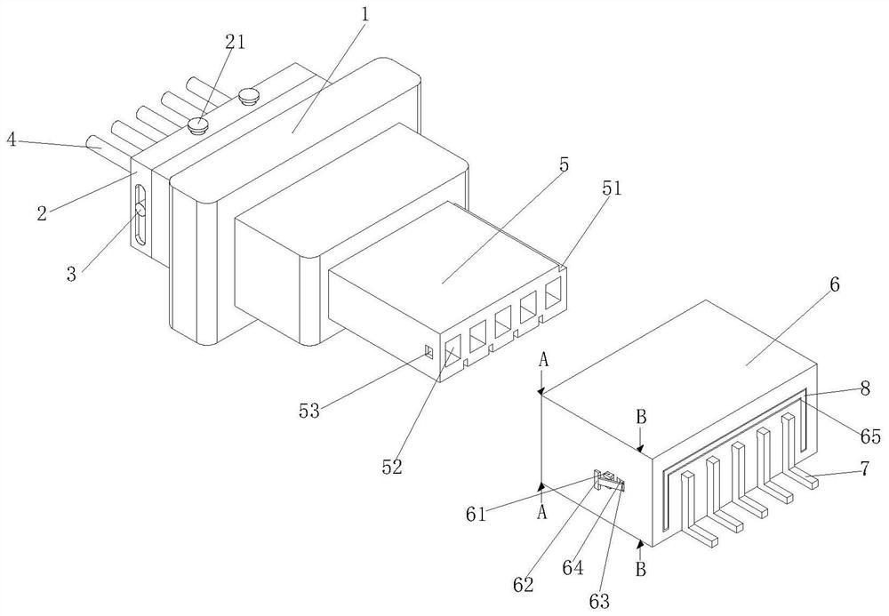
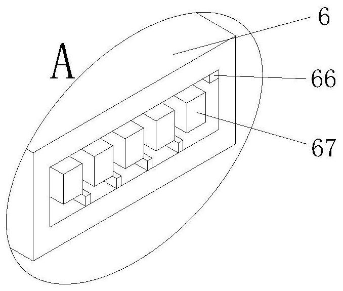
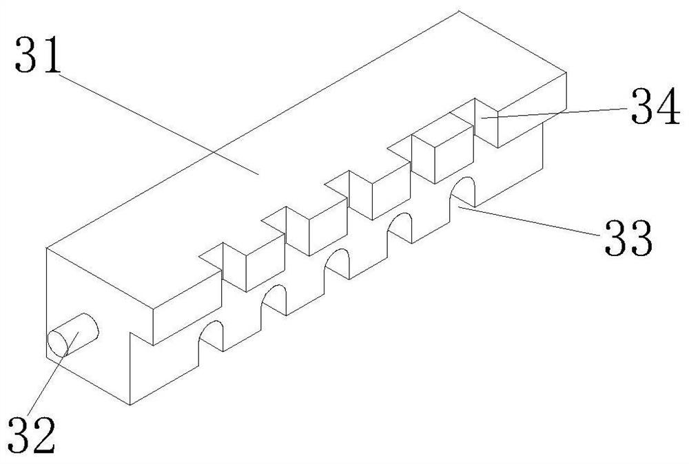
[0022] The following will clearly and completely describe the technical solutions in the embodiments of the present invention with reference to the accompanying drawings in the embodiments of the present invention. Obviously, the described embodiments are only some, not all, embodiments of the present invention.

[0023] Examples of the described embodiments are shown in the drawings, wherein like or similar reference numerals designate like or similar elements or elements having the same or similar functions throughout. The embodiments described below by referring to the figures are exemplary and are intended to explain the present invention and should not be construed as limiting the present invention.

[0024] In describing the present invention, it should be understood that the terms "center", "longitudinal", "transverse", "length", "width", "thickness", "upper", "lower", "front", " Back", "Left", "Right", "Vertical", "Horizontal", "Top", "Bottom", "Inner", "Outer", "Clock...


PUM


Abstract

The invention discloses a chip packaging connector assembly, which comprises a connecting head mounting plate, a wire harness pressing plate, a connecting head, a connecting seat, pins and a dustproof board. In the present invention, a wire harness pressure plate is arranged at the wire harness, the wire harness is bent and the connector mounting plate is fixed through the wire harness guide groove, and the wire harness and the bottom end of the substrate are fixed through the wire harness pressure groove, so as to prevent local stress on the fixed part of the wire harness and the connector mounting plate , causing the circuit to be disconnected, and at the same time it is convenient to bundle the wire harness, and a damper installation groove is set inside the connection seat, and a damper is arranged inside the damper installation groove, and the connector and the connection seat are snapped and fixed so that the dustproof board can be separated from the dustproof board installation groove Stretch out and fix, the inner spring of the damper is compressed, the connecting head is separated from the connecting seat, the inner spring of the damper stretches, drives the dust-proof plate to retract into the installation groove of the dust-proof plate, and makes the connecting head pop out from the connecting seat.

Description

technical field [0001] The invention relates to the technical field of chip packaging, in particular to a chip packaging connector assembly. Background technique [0002] Electronic chip packaging has long used multiple modes for sending and receiving information between the die contained in the package and the electronics outside the package, electronic interconnects provide the die in the package and can be used from and to the die An electrical connection between various communication components that send and receive electronic signals, one such communication component being the conventional header-attached solder bumps configured to pass through a motherboard or other circuit board between a package and another electronic device Creates a physical electrical connection. Another such communication component is a cable connector that allows communication between the die and external electronics without the need for a motherboard. Existing chip package connectors are snap-f...

Claims


Application Information

Patent Timeline
Patent Type & Authority Patents(China)
IPC IPC(8): H01R13/58H01R13/52H01R13/635H01R12/70
CPCH01R12/707H01R13/52H01R13/5812H01R13/635
Inventor 史少峰阮怀其
Owner 安徽国晶微电子有限公司
Why Eureka
Try Eureka