PCB electroplating device

An electroplating device and electroplating solution technology, applied in the direction of plating tanks, electrolytic processes, electrolytic components, etc., can solve problems such as energy waste, achieve the effects of saving energy waste, increasing flow rate and flow, and increasing deep plating capacity

Active Publication Date: 2019-12-31
DONGGUAN SHENGYI ELECTRONICS
View PDF5 Cites 3 Cited by
  • Summary
  • Abstract
  • Description
  • Claims
  • Application Information

AI Technical Summary

Problems solved by technology

[0009] The purpose of the present invention is to provide a PCB electroplating device to solve the problem of increasing the jet flow vertically and parallel to the PCB surface when making PCBs with a thickness-to-diameter ratio of 16:1 and above 16:1 in the prior art. To improve this, it is necessary to use a higher power pump, and the problem of serious energy waste

Method used


Image

  • PCB electroplating device
  • PCB electroplating device
  • PCB electroplating device

Examples


Embodiment Construction

[0037] The technical solutions of the present invention will be further described below in conjunction with the accompanying drawings and through specific implementation methods.

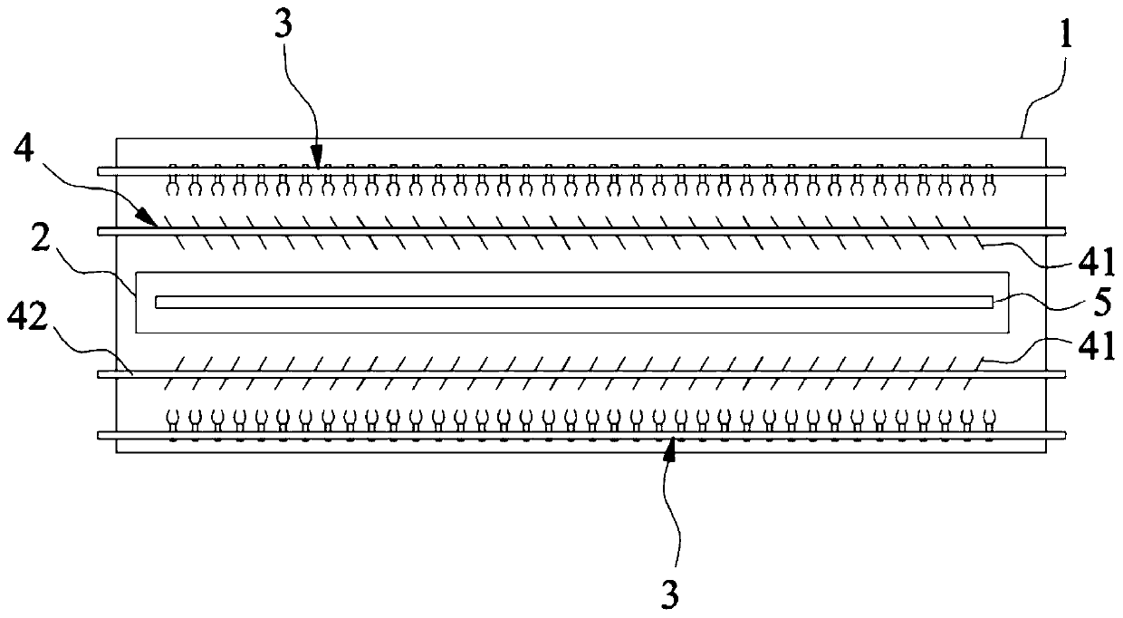
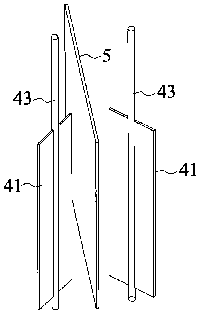
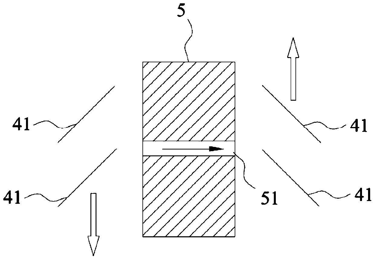
[0038] Such as Figure 1~4 As shown, this embodiment provides a PCB electroplating device, which includes an electroplating tank 1 , a fixture 2 , two anodes 3 and a spoiler assembly 4 . The electroplating tank 1 is used to accommodate the electroplating solution. The fixture 2 is used to clamp the PCB5, and can make the PCB5 be immersed in the electroplating solution along the vertical direction. Both anodes 3 are configured to be immersed in the electroplating solution and are respectively located on two sides of the PCB 5 . The spoiler assembly 4 is configured to be immersed in the electroplating solution, and the spoiler assembly 4 can push the electroplating solution from one side of the PCB5 through the drill hole 51 on the PCB5 to the other side of the PCB5. In this embodiment, the electro...


PUM

PropertyMeasurementUnit
angleaaaaaaaaaa
widthaaaaaaaaaa
lengthaaaaaaaaaa

Abstract

The invention relates to the technical field of PCB electroplating and particularly discloses a PCB electroplating device. The PCB electroplating device comprises an electroplating bath, a clamp, twopositive poles and turbulent flow components. The clamp is used for clamping a PCB and immersing the PCB in an electroplating solution in the electroplating bath in the vertical direction, the two positive poles are placed on both sides of the PCB, and the turbulent flow components are located between the PCB and one of the positive poles. Each turbulent flow component comprises a blade frame andblades mounted on the blade frame. The blade frames drive the blades to swing in a reciprocating manner parallel to the PCB faces in the horizontal direction, and the blades push the electroplating solution, so that a pressure difference is generated between the two plate faces of the PCB, the plating solution is promoted to flow through a drilling hole in the PCB, the flow rate of the plating solution passing through the drilling hole is increased, and the deep plating capacity of the drilling hole is improved; and compared with the prior art, by the adoption of the PCB electroplating device,the deep plating capacity of the PCB with the thickness ratio of equal to or greater than 16:1 can be remarkably improved, higher-power pumping is not needed, and energy waste is relatively saved,

Description

technical field [0001] The invention relates to the technical field of PCB electroplating, in particular to a PCB electroplating device. Background technique [0002] With the development of 5G mobile communication technology, the explosive growth of communication data has promoted the continuous increase of communication PCB layers and the continuous decrease of aperture, which in turn leads to the PCB thickness-to-diameter ratio (PCB board thickness / PCB minimum drilling aperture) From 12:1 in the 3G and 4G era to 20:1 or even 25:1, and the thickness-to-diameter ratio of 16:1 and above has become a typical feature of 5G communication PCBs. [0003] 5G mobile communication equipment has high requirements on the reliability and graphic accuracy of PCB, and the deep plating ability of electroplating has a direct impact on these two indicators. Higher deep plating ability can not only ensure that the copper layer in the PCB hole reaches a sufficient thickness, In order to ensu...

Claims


Application Information

Patent Timeline
Patent Type & Authority Applications(China)
IPC IPC(8): C25D7/00C25D17/02C25D17/06C25D21/10C25D5/08
CPCC25D5/08C25D7/00C25D17/02C25D17/06C25D21/10
Inventor 袁继旺曹大福周宜洛
Owner DONGGUAN SHENGYI ELECTRONICS
Why Eureka
Try Eureka