Monocrystalline silicon slicing device capable of freely adjusting size of wafer to be cut

A technology of slicing device and single crystal silicon, which is applied to fine working devices, stone processing equipment, manufacturing tools, etc., can solve the problems of incomplete fixation, waste of production resources, and easy movement during single crystal silicon cutting, so as to increase the Practicality, saving resources, and ensuring the effect of production quality

Inactive Publication Date: 2020-01-03
江苏晶品新能源股份有限公司
View PDF0 Cites 2 Cited by
  • Summary
  • Abstract
  • Description
  • Claims
  • Application Information

AI Technical Summary

Problems solved by technology

[0002] Single crystal of silicon, a crystal with a basically complete lattice structure, has different properties in different directions, is a good semiconductor material, used to manufacture semiconductor devices, solar cells, etc., the existing single crystal silicon is being processed and produced , it is necessary to cut a large volume of monocrystalline silicon into small parts, but the existing cutting device can only cut monocrystalline silicon into one size, which has great limitations, and the monocrystalline silicon is fixed during cutting. If it is not thorough, it is easy to move, causing cutting errors and wasting production resources. Therefore, we propose a single crystal silicon slicing device that can freely adjust the size of the cut wafer

Method used


Image

  • Monocrystalline silicon slicing device capable of freely adjusting size of wafer to be cut
  • Monocrystalline silicon slicing device capable of freely adjusting size of wafer to be cut
  • Monocrystalline silicon slicing device capable of freely adjusting size of wafer to be cut

Examples


Embodiment Construction

[0018] The following will clearly and completely describe the technical solutions in the embodiments of the present invention with reference to the accompanying drawings in the embodiments of the present invention. Obviously, the described embodiments are only some, not all, embodiments of the present invention. Based on the embodiments of the present invention, all other embodiments obtained by persons of ordinary skill in the art without making creative efforts belong to the protection scope of the present invention.

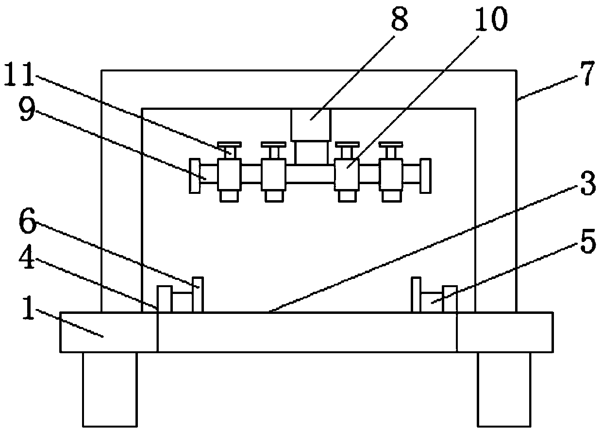
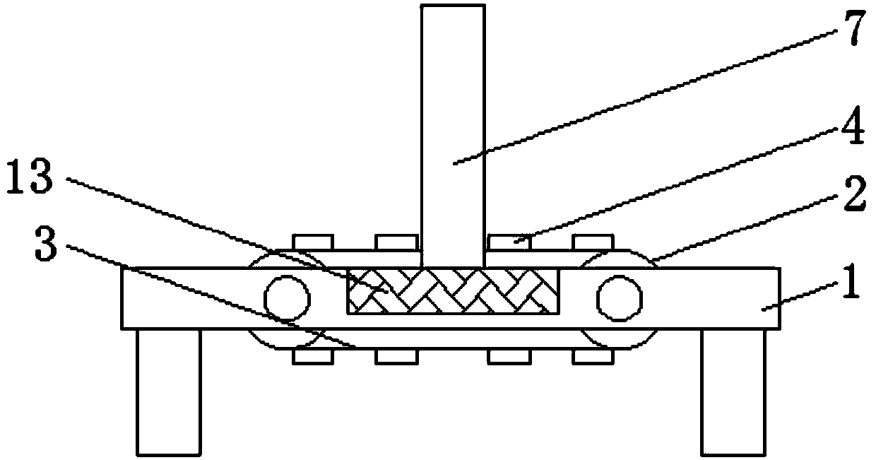
[0019] see Figure 1-4 , the present invention provides a technical solution: a single crystal silicon slicing device that can freely adjust the size of the cut wafer, including a working platform 1, the working platform 1 is a square hollow working platform, and two One set of guide rollers 2, two sets of guide rollers 2 are driven by the conveyor belt 3, and the surface of the conveyor belt 3 is evenly opened with holes, which facilitates the scrap impuritie...


PUM


Abstract

The invention discloses a monocrystalline silicon slicing device capable of freely adjusting size of a wafer to be cut, and belongs to the technical field of monocrystalline silicon. The slicing device comprises a working platform, wherein two groups of guide rollers are driven by a conveyor belt, a chip collecting box is installed in the center of an inner cavity of the working platform, and theend, away from fixing blocks, of a supporting rod is connected with a clamping device; and an electric telescopic rod is arranged in the center of the bottom of a rack, the bottom of the electric telescopic rod is connected with a fixing rod, the outer wall of the fixing rod is uniformly sleeved with sleeves, and cutting blades are arranged in the centers of the bottoms of the sleeves. The spacingbetween the sleeves is adjusted in the device, so that the device can cut the monocrystalline silicon into different sizes; the monocrystalline silicon is fixed by the clamping device, so that cutting exists in errors caused by the movement of the monocrystalline silicon are prevented; and meanwhile, the cutting blades rotate, so that blocking blocks rotate like fan blades to generate wind force,and chips generated by cutting on the working platform are blown to the chip collecting box, and the chips are prevented from splashing onto the monocrystalline silicon to damage the surface of the monocrystalline silicon.

Description

technical field [0001] The invention relates to the technical field of monocrystalline silicon, in particular to a monocrystalline silicon slicing device which can freely adjust the size of a cut wafer. Background technique [0002] Single crystal of silicon, a crystal with a basically complete lattice structure, has different properties in different directions, is a good semiconductor material, used to manufacture semiconductor devices, solar cells, etc., the existing single crystal silicon is being processed and produced , it is necessary to cut a large volume of monocrystalline silicon into small parts, but the existing cutting device can only cut monocrystalline silicon into one size, which has great limitations, and the monocrystalline silicon is fixed during cutting. If it is not thorough, it is easy to move, causing cutting errors and wasting production resources. Therefore, we propose a single crystal silicon slicing device that can freely adjust the size of the cut ...

Claims


Application Information

Patent Timeline
Patent Type & Authority Applications(China)
IPC IPC(8): B28D5/02B28D5/00
CPCB28D5/0076B28D5/0082B28D5/029
Inventor 陈春成戚建静
Owner 江苏晶品新能源股份有限公司
Why Eureka
Try Eureka