A Polarizing Beam Splitter with Large Fabrication Tolerance and High Polarization Extinction Ratio

A technology of polarization beam splitter and polarization extinction ratio, which is applied in the direction of instruments, light guides, optics, etc., can solve the problems of small manufacturing tolerance, hindering the large-scale application of single-chip integrated coherent receivers, and increasing the difficulty of manufacturing due to the device structure. To achieve the effect of improving production tolerance

Active Publication Date: 2021-01-26
HUAZHONG UNIV OF SCI & TECH
View PDF18 Cites 0 Cited by
  • Summary
  • Abstract
  • Description
  • Claims
  • Application Information

AI Technical Summary

Problems solved by technology

However, the complex device structure increases the difficulty of fabrication, and the wavelength dependence of the quantum-confined Stark effect makes the polarization extinction ratio of this scheme unable to meet the application requirements in the C-band
[0004] In summary, the polarization extinction ratio of today's polarization beam splitters cannot meet the application requirements, and the manufacturing tolerance is small, which hinders the large-scale application of monolithic integrated coherent receivers

Method used


Image

  • A Polarizing Beam Splitter with Large Fabrication Tolerance and High Polarization Extinction Ratio
  • A Polarizing Beam Splitter with Large Fabrication Tolerance and High Polarization Extinction Ratio
  • A Polarizing Beam Splitter with Large Fabrication Tolerance and High Polarization Extinction Ratio

Examples


example 1

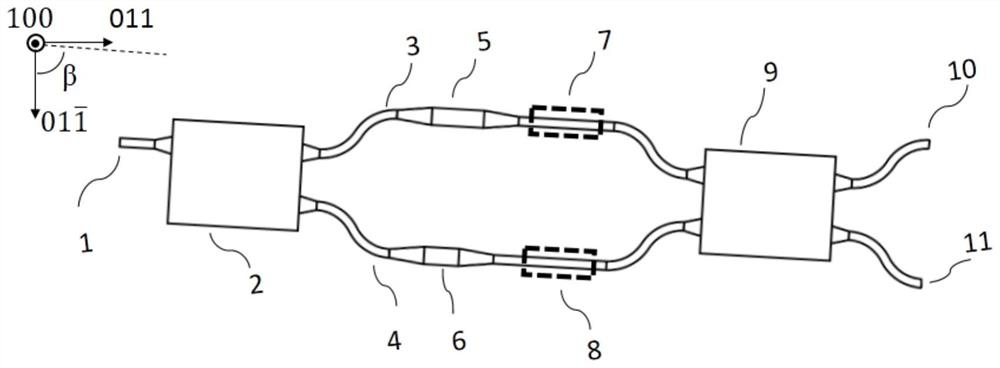
[0042] Example 1 The thickness of the selected waveguide core layer is 0.4 μm, the material is InGaAsP, the width is 2 μm, the waveguide substrate and cover layer are InP, the length of the phase shift waveguide is 2.5mm, and the incident wavelength is 1550nm. The waveguide is oriented with the crystal's The angle β of the direction is 90°, and the width of the waveguide in the birefringent region is consistent with that of the straight waveguide, such as figure 2 shown.

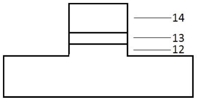
[0043] The waveguide adopts the structure of P-I-N type. image 3 It is a cross-sectional view of the P-I-N waveguide structure, from bottom to top there are N-type doped waveguide substrate 12, undoped waveguide core layer 13 and P-type doped waveguide cover layer 14.

[0044] First, we specifically analyze the first-order electro-optic effect, the second-order electro-optic effect, the carrier dispersion effect and the energy band filling effect.

[0045] The first-order electro-optic effect means tha...

example 2

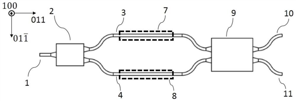
[0075] In Example 2, the thickness of the waveguide core layer selected is 0.4 μm, the material is InGaAsP, and the width is 2 μm. The waveguide substrate and cover layer are InP. There is a 1.5um thick InGaAs spacer layer at 2 μm below the waveguide core layer. The length of the phase shift waveguide is 2.5mm, the incident wavelength is 1550nm, the upper arm waveguide covers the thermal electrode 15 and the lower arm waveguide electrode 16 . The waveguide is oriented with the crystal's The angle β of the direction is 90°, such as Figure 9 shown.

[0076] The waveguide adopts the structure of P-I-N type. Figure 10 It is a cross-sectional view of the P-I-N waveguide structure. From bottom to top, there are N-type doped waveguide substrate 17, N-type doped spacer layer 18, undoped waveguide core layer 19 and P-type doped waveguide cover layer. 20.

[0077] The heating of the thermal electrode 15 of the upper arm waveguide can change the effective refractive index of the T...


PUM

PropertyMeasurementUnit
thicknessaaaaaaaaaa
widthaaaaaaaaaa

Abstract

The invention discloses a polarization beam splitter with large manufacturing tolerance and high polarization extinction ratio. The polarization beam splitter includes an input waveguide, a multimode interference coupler, two phase shift waveguides, Mode interference coupler and output waveguide; the multimode interference coupler divides the light intensity of the input waveguide equally, enters the upper and lower two phase shift waveguides respectively, and then outputs through 2×2 multimode interference coupler interference. The direction of the waveguide and the direction of the crystal have an included angle of 45-135 degrees. By applying a voltage on the two phase-shifting waveguides, the effective refractive index of TE and TM polarized light is changed respectively, so that the phases of TE and TM polarized light meet the interference constructive and destructive conditions of 2×2MMI respectively, and polarization beam splitting is realized. The present invention compensates the extra phase difference of polarized light caused by manufacturing process deviation by changing the effective refractive index of TE and TM polarized light, so it has a large manufacturing tolerance; in addition, because 2×2MMI can achieve a very high extinction ratio, the present invention The inventive polarizing beam splitter has a high polarization extinction ratio.

Description

technical field [0001] The invention relates to an optical component, in particular to a polarization beam splitter. Background technique [0002] With the continuous improvement of optical communication transmission rate requirements, the traditional amplitude modulation method can no longer meet the upgrading requirements of the communication network. The quadrature phase shift modulation format of polarization multiplexing is widely used, and the signal demodulation method is also upgraded from the traditional direct detection. for coherent detection. At the same time, the development trend of miniaturization, low power consumption and low cost of optical communication devices requires the integration of optical devices with different functions. Therefore, the single-chip integrated dual-polarization quadrature phase-shift keying receiver becomes very important, and the inability to realize high-performance waveguide polarization beam splitter is the main reason hinderin...

Claims


Application Information

Patent Timeline
Patent Type & Authority Patents(China)
IPC IPC(8): G02B6/126G02B6/125G02B6/12G02F1/015G02F1/025G02F1/01
CPCG02B6/12004G02B6/125G02B6/126G02B2006/12147G02B2006/1215G02F1/011G02F1/0147G02F1/015G02F1/025G02F1/0151
Inventor 陆巧银戴向阳陈泉安马向国伟华
Owner HUAZHONG UNIV OF SCI & TECH
Why Eureka
Try Eureka