Bidirectional ESD protection device

An ESD protection and device technology, applied in the direction of electric solid devices, semiconductor devices, electrical components, etc., can solve the problems of uneven stress and voltage consistency of chips, improve the voltage consistency and reliability of devices, improve voltage consistency, High reliability effect

Pending Publication Date: 2020-01-03
江苏吉莱微电子股份有限公司
View PDF0 Cites 2 Cited by
  • Summary
  • Abstract
  • Description
  • Claims
  • Application Information

AI Technical Summary

Problems solved by technology

[0004] The invention solves the problems of chip stress unevenness and voltage consistency

Method used


Image

  • Bidirectional ESD protection device
  • Bidirectional ESD protection device
  • Bidirectional ESD protection device

Examples


Embodiment Construction

[0025] The present invention will be described in further detail below in conjunction with the accompanying drawings and embodiments.

[0026] The technical solution described in the present invention is only a part of the embodiments of the present invention. Based on the invention proposed by adding a charge control area in the isolation groove of the vertical triode to adjust the electric field to achieve the purpose of controlling the voltage of the triode and related other embodiments, all Belong to the protection scope of the present invention.

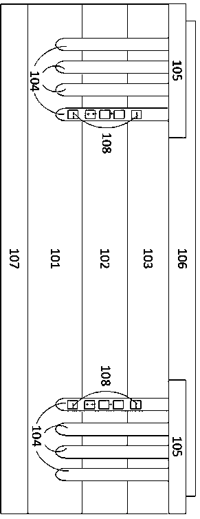
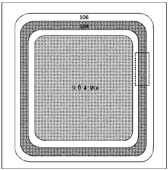
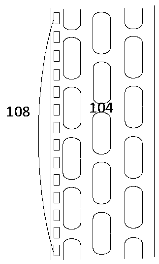
[0027] Such as figure 1 As shown, a bidirectional ESD protection device has a structure comprising: an N+ substrate layer 101, a P-type epitaxial layer 102 above the N+ substrate layer 101, and an N+ doped layer 103 above the P-type epitaxial layer 102. The combination of the N+ substrate layer 101 , the P-type epitaxial layer 102 and the N+ doped layer 103 forms a vertical triode structure. The deep isolation trenches 104 are...


PUM


Abstract

A bidirectional ESD protection device is a chip composed of an N+ substrate layer 101, a P-type epitaxial layer 102 and an N+ doped layer 103. The P-type epitaxial layer 102 is arranged above the N+ substrate layer 101, and the N+ doped layer 103 is arranged above the P-type epitaxial layer 102. Deep isolation grooves 104 are formed in the left side and the right side of the chip; a doped polycrystalline floating island 108 is arranged in the deep isolation groove 104 close to the central area of the chip; an isolation dielectric layer 105 is arranged between the deep isolation groove 104 anda front electrode 106; the front electrode 106 is arranged above the N+ doped layer 103 and the isolation dielectric layer 105; and a back electrode 107 is formed below the N+ substrate layer 101. Aiming at ESD protection applied to common capacitance and large current discharge capacity, a trench gate-isolated longitudinal triode structure is adopted, and the electrostatic discharge problem of anintegrated circuit is solved.

Description

technical field [0001] The invention belongs to the field of electronic science and technology, and mainly relates to the field of integrated circuit electrostatic discharge (ESD-Electrostatic Discharge) protection, in particular to a bidirectional ESD protection device. Background technique [0002] Electrostatic discharge (ESD) phenomenon widely exists in the daily environment, it is indeed a fatal threat to precision integrated circuits, and it is one of the important reasons for damage or even failure of integrated circuit products. Integrated circuit products are extremely vulnerable to ESD during their production, manufacturing, assembly and working process, resulting in internal damage and reduced reliability of the product. And its application environment will also have corresponding requirements for parameters such as capacitance, breakdown voltage, and clamping characteristics. [0003] For different applications, the system has different requirements on the param...

Claims


Application Information

Patent Timeline
IPC IPC(8): H01L27/02
CPCH01L27/0262
Inventor 张鹏杨钰琳宋文龙
Owner 江苏吉莱微电子股份有限公司
Why Eureka
Try Eureka