Method for preparing indium bumps of reading circuit of infrared detector

A technology for infrared detectors and readout circuits, which is applied in the direction of circuits, semiconductor/solid-state device manufacturing, electrical components, etc., can solve the problems of inability to prepare high-uniformity indium bumps, and achieve low preparation difficulty and high uniformity Effect

Active Publication Date: 2020-01-07
11TH RES INST OF CHINA ELECTRONICS TECH GROUP CORP
View PDF7 Cites 13 Cited by
  • Summary
  • Abstract
  • Description
  • Claims
  • Application Information

AI Technical Summary

Problems solved by technology

Due to the continuous reduction of pixel center spacing, the traditional method of preparing indium bumps by peeling off has been unable to prepare indium bumps with high uniformity and high requirements

Method used


Image

  • Method for preparing indium bumps of reading circuit of infrared detector
  • Method for preparing indium bumps of reading circuit of infrared detector
  • Method for preparing indium bumps of reading circuit of infrared detector

Examples


preparation example Construction

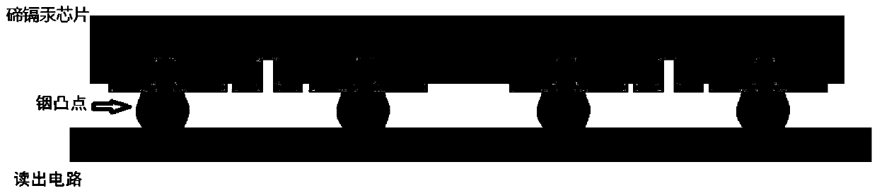
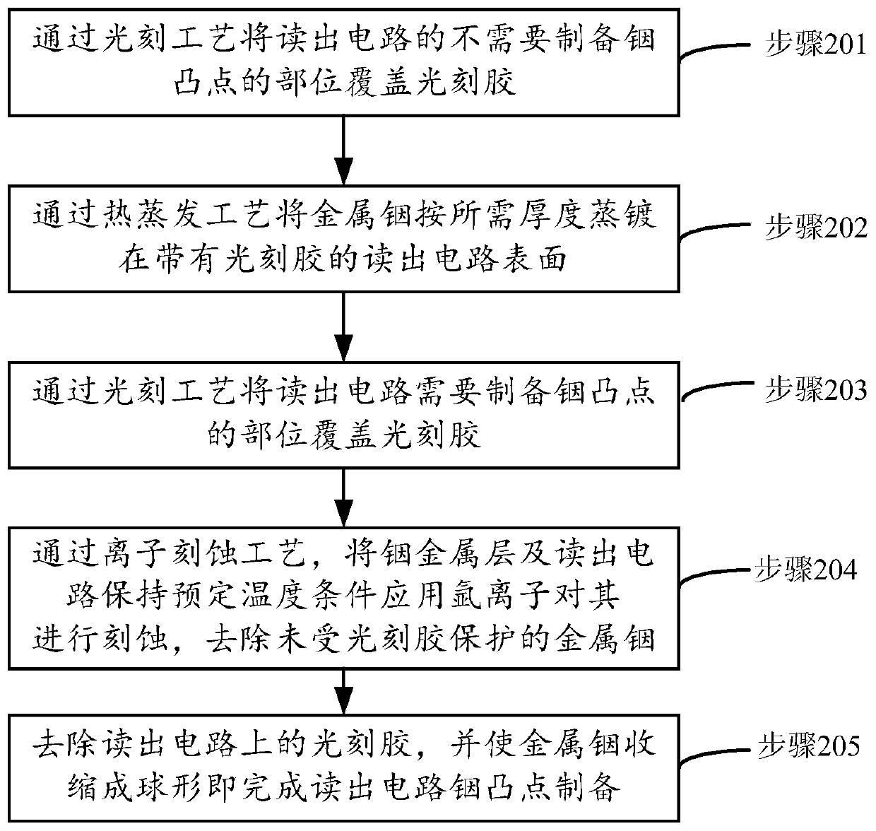
[0025] According to an embodiment of the present invention, a method for preparing an indium bump for an infrared detector readout circuit is provided, figure 2 It is a flow chart of the method for preparing an indium bump for an infrared detector readout circuit according to an embodiment of the present invention, such as figure 2 As shown, the method for preparing an indium bump for an infrared detector readout circuit according to an embodiment of the present invention specifically includes:

[0026] Step 201 , covering the parts of the readout circuit that do not require indium bumps with photoresist through a photolithography process; wherein, the thickness of the photoresist covering the parts that do not need indium bumps is 1 μm.

[0027] Step 202, evaporating metal indium on the surface of the readout circuit with photoresist according to the required thickness by thermal evaporation process;

[0028] Step 203, covering the parts of the readout circuit where indium...


PUM

PropertyMeasurementUnit
thicknessaaaaaaaaaa

Abstract

The invention discloses a method for preparing indium bumps of a reading circuit of an infrared detector. The method comprises steps of covering photoresist on a part, which does not need to be provided with indium bumps, of the reading circuit through the photoetching process; evaporating metal indium on a surface of the reading circuit with the photoresist according to the required thickness through the thermal evaporation process; covering photoresist on the part of the reading circuit, which needs to be provided with the indium bumps, through the photoetching process; through the ion etching process, etching the indium metal layer and the reading circuit by using argon ions while keeping the preset temperature condition, and removing the metal indium which is not protected by the photoresist; and removing the photoresist on the reading circuit, and shrinking the metal indium into a sphere to finish preparation of the indium bumps of the reading circuit.

Description

technical field [0001] The invention relates to the technical field of semiconductor circuit processing in microelectronic technology, in particular to a method for preparing indium bumps of an infrared detector readout circuit. Background technique [0002] Infrared focal plane detection technology has significant advantages such as wide spectral response band, more ground target information can be obtained, and can work day and night. It is widely used in early warning detection, intelligence reconnaissance, damage effect assessment, and investigation, development and Management, weather forecast, geothermal distribution, earthquake, volcanic activity, space astronomical exploration and other fields. [0003] HgCdTe infrared detector is one of the representative products of infrared detection technology. With the advancement of technology, the size of the area array of HgCdTe infrared detectors has been continuously developed, and the distance between the center of the pi...

Claims


Application Information

Patent Timeline
Patent Type & Authority Applications(China)
IPC IPC(8): H01L21/60H01L31/101
CPCH01L24/11H01L24/14H01L31/101
Inventor 张轶刘世光孙浩刘震宇
Owner 11TH RES INST OF CHINA ELECTRONICS TECH GROUP CORP
Why Eureka
Try Eureka