an optical device

An optical device and visible light technology, applied in the field of infrared optics, can solve the problems such as the difficulty of controllable adjustment of white light power and the difficulty of perfectly presenting visual effects, and achieve the effects of strong anti-interference ability, reduced packaging costs, and soft visual effects.

Active Publication Date: 2021-05-04
GRIREM ADVANCED MATERIALS CO LTD
View PDF4 Cites 0 Cited by
  • Summary
  • Abstract
  • Description
  • Claims
  • Application Information

AI Technical Summary

Problems solved by technology

At present, the main problems of this implementation method are: the power of near-infrared luminous light still needs to be further improved, and it is difficult to achieve controllable adjustment of the light power of white light, and it is difficult to perfectly present a soft visual effect

Method used


Image

  • an optical device
  • an optical device
  • an optical device

Examples


Embodiment 1

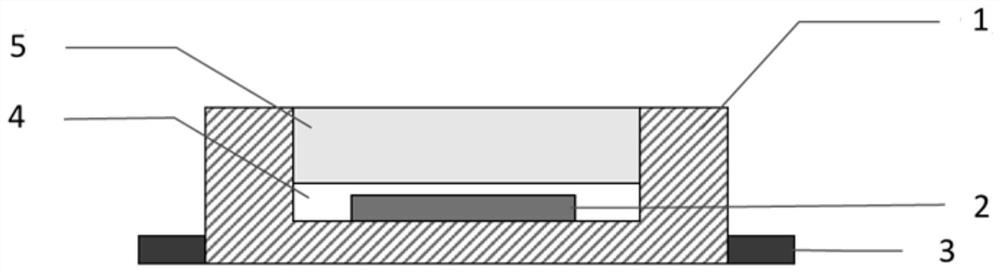
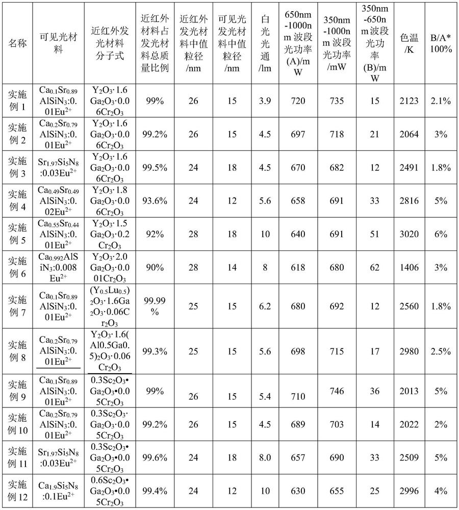
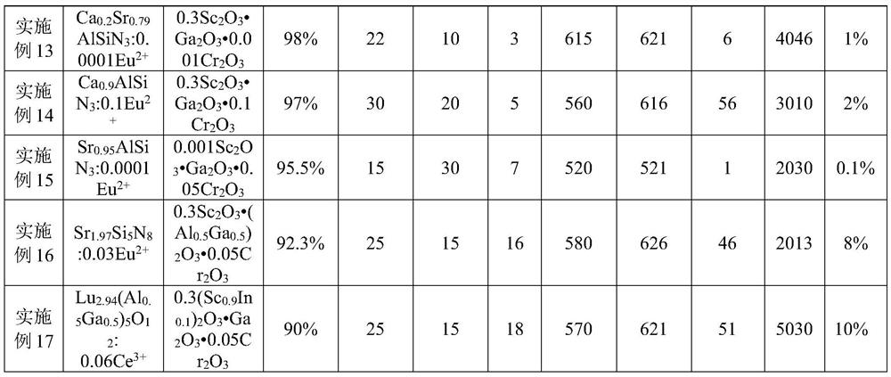
[0056] An optical device, the components of which are blue LED chips with a wavelength of 440nm and a molecular formula of Ca 0.1 Sr 0.89 AlSiN 3 :0.01Eu 2+ Visible light luminescent material, the molecular formula is Y 2 o 3 1.6Ga 2 o 3 0.06Cr 2 o 3 The near-infrared luminescent material; wherein the near-infrared luminescent material accounts for 99% of the total mass of the luminescent material, and the D50 particle size of the near-infrared luminescent material is 26 μm; the D50 particle size of the visible light luminescent material is 15 μm. Mix the visible light luminescent material and silica gel evenly in the present invention, stir and defoam to obtain the visible light fluorescence conversion layer mixture, and cover the mixture on the surface of the LED chip layer by coating, wherein the visible light luminescent material is on the light emitting surface of the LED chip The coating mass in the vertical direction accounts for 20% of the total mass of the vis...

Embodiment 4

[0059] An optical device, the components of which are blue LED chips with a wavelength of 460nm and a molecular formula of Ca 0.49 Sr 0.49 AlSiN 3 :0.02Eu 2+ Visible light luminescent material, the molecular formula is Y 2 o 3 1.8Ga 2 o 3 0.06Cr 2 o 3 The near-infrared luminescent material; wherein the near-infrared luminescent material accounts for 93.6% of the total mass of the luminescent material, and the D50 particle size of the near-infrared luminescent material is 24 μm; the D50 particle size of the visible light luminescent material is 12 μm. Mix the visible light luminescent material and silica gel evenly in the present invention, stir and defoam to obtain the visible light fluorescence conversion layer mixture, and cover the mixture on the surface of the LED chip layer by dispensing, wherein the visible light luminescent material is on the light emitting surface of the LED chip The coating mass in the vertical direction accounts for 10% of the total mass of t...

Embodiment 7

[0062] An optical device, the components of which are blue LED chips with a wavelength of 420nm and a molecular formula of Ca 0.1 Sr 0.89 AlSiN 3 :0.01Eu 2+ Visible light luminescent material, the molecular formula is (Y 0.5 Lu 0.5 ) 2o 3 1.6Ga 2 o 3 0.06Cr 2 o 3 The near-infrared luminescent material; wherein the near-infrared luminescent material accounts for 99.99% of the total mass of the luminescent material, and the D50 particle size of the near-infrared luminescent material is 25 μm; the D50 particle size of the visible light luminescent material is 15 μm. Mix the visible light luminescent material and silica gel evenly in the present invention, stir and defoam to obtain the visible light fluorescence conversion layer mixture, and cover the mixture on the surface of the LED chip layer by dispensing, wherein the visible light luminescent material is on the light emitting surface of the LED chip The coating mass in the vertical direction accounts for 10% of the ...


PUM

PropertyMeasurementUnit
wavelengthaaaaaaaaaa
particle sizeaaaaaaaaaa

Abstract

An optical device, the optical device includes an LED chip, a visible light emitting material, and a near-infrared light emitting material, wherein the near-infrared and visible light emitting materials emit a 650-1000nm band optical power under excitation by the LED chip. The sum of the optical power emitted in the 350-650nm band under the excitation of the LED chip, and the residual emitted optical power of the LED chip in the 350-650nm band after the near-infrared and visible light emitting materials are excited by the LED chip, is B, where B / A* 100% is 0.1%‑10%. The optical device utilizes the realization method of simultaneously compounding near-infrared light-emitting materials and visible light-emitting materials with LED chips, realizes near-infrared and visible light emission simultaneously with the same LED chip, and obtains strong near-infrared light emission and weak visible light emission, and the device is extremely The packaging process is simplified, the packaging cost is reduced, the luminous efficiency is high, the reliability is excellent, and there is no red explosion, and the optical power, especially the white light optical power, can be controlled and adjusted, and finally a soft visual effect can be achieved.

Description

technical field [0001] The invention relates to the technical field of infrared optics, in particular to optical devices of LED chips, visible light luminescent materials and near-infrared luminescent materials. Background technique [0002] In recent years, the application of near-infrared light in the fields of security monitoring, biometrics, 3D sensing, and food / medical testing has become a focus at home and abroad. Among them, near-infrared LED has become an international research hotspot because of its good directivity, low power consumption and small size. At present, the main implementation method of near-infrared LED is to use near-infrared semiconductor chips. For example, in the field of security, infrared chips with 730nm, 750nm, 850nm and 940nm bands are mainly used, especially short-wave infrared chips will produce very serious redness during use. Usually, one or more white LEDs are installed externally to compensate the light in the dark detection process and...

Claims


Application Information

Patent Timeline
Patent Type & Authority Patents(China)
IPC IPC(8): H01L33/50
CPCH01L33/504H01L2933/0041
Inventor 刘荣辉刘元红陈晓霞薛原马小乐
Owner GRIREM ADVANCED MATERIALS CO LTD
Why Eureka
Try Eureka