Method for manufacturing isolation structure of semiconductor device and semiconductor device thereof

A device isolation and semiconductor technology, applied in semiconductor lasers, laser components, instruments, etc., can solve problems such as inability to complete lift-off operations

Active Publication Date: 2020-01-07
深圳市矽赫科技有限公司
View PDF8 Cites 0 Cited by
  • Summary
  • Abstract
  • Description
  • Claims
  • Application Information

AI Technical Summary

Problems solved by technology

However, the lift-off requires the photoresist to fully contact the solvent. In the traditional process, after we evaporate at an angle, both sides of the photoresist "wall" are covered with metal, and the solvent cannot be immersed, so the lift-off operation cannot be completed.

Method used


Image

  • Method for manufacturing isolation structure of semiconductor device and semiconductor device thereof
  • Method for manufacturing isolation structure of semiconductor device and semiconductor device thereof
  • Method for manufacturing isolation structure of semiconductor device and semiconductor device thereof

Examples


Embodiment 1

[0037] This embodiment provides a semiconductor device, which is manufactured by the following method:

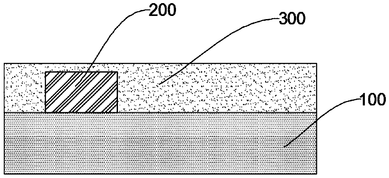
[0038] (1) providing a substrate 100;

[0039] (2) forming the device 200 on the substrate 100;

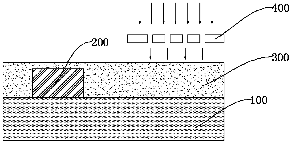
[0040] (3) Forming a conductive isolation structure 700 on the substrate 100 .

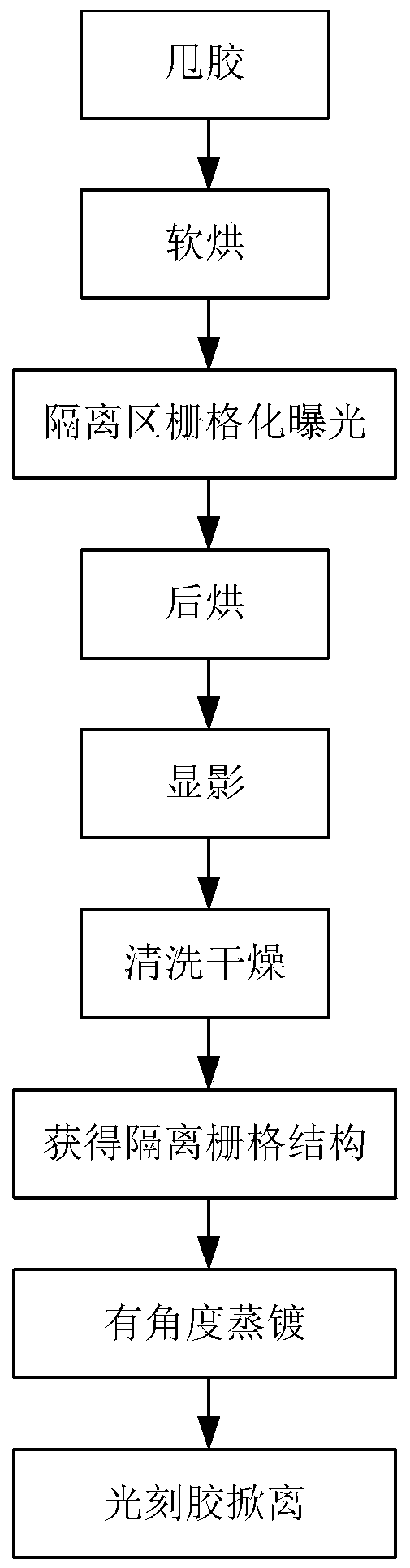
[0041] according to figure 1 As shown, the method wherein the conductive isolation structure 700 is formed includes the following steps:

[0042] (1) Forming the photoresist layer 300 on the device 200 and the substrate 100 , the method for forming the photoresist layer 300 includes performing photoresist spinning on the upper surfaces of the device 200 and the substrate 100 after etching. In this embodiment, the photoresist is a negative photoresist, the model is Su-8 3005 from MicroChem, the thickness of the formed photoresist layer 300 is 7 μm, and the speed of spinning the photoresist is 2000 rpm.

[0043] (2) Baking the photoresist layer 300 after the spun-off is performed to remove the so...

Embodiment 2

[0054] The difference from Embodiment 1 is that in the manufacturing method of the semiconductor device provided in this embodiment, the substrate 100 and the device 200 are exposed to the photoresist layer 300 without masking after removing the photoresist layer 300. Thus, the first structure 500 is formed in the photoresist layer 300 .

[0055] The photoresist in this embodiment is a negative photoresist, and the exposure treatment adopted is exposure treatment using interference light.


PUM


Abstract

The invention relates to semiconductor manufacturing, in particular to a method for manufacturing the isolation structure of a semiconductor device and a semiconductor device. The manufacturing process of the semiconductor device includes the following steps that: a substrate is provided; a device is formed on the substrate; and a conductive isolation structure is formed on the substrate. The method for forming the conductive isolation structure comprises the following steps that: a photoresist layer is formed on the device and the substrate; a grid structure is formed in the photoresist layer; the grid structure is reserved; a conductive layer is formed on the surfaces of the device, the substrate and the grid structure; and the grid structure is lifted off. According to the method of theinvention, a lift-off process is provided; the photoresist with a lift-off function is subjected to gridding treatment, so that the photoresist can still be in full contact with a solvent after a sample piece is subjected to angled evaporation, and lift-off operation is completed.

Description

technical field [0001] The invention relates to semiconductor manufacturing, in particular to a method for manufacturing an isolation structure of a semiconductor device and a semiconductor device thereof. Background technique [0002] Among semiconductor lasers, many linear micro-lasers are three-dimensional micro-wall structures. The width of the top of these wall structures is on the order of microns, and the structure is fragile. It is difficult to directly use the top of the wall as a conductive contact area in both testing and practical applications. . Therefore, generally, a conductive layer is plated on the surface of the entire wall structure, the top is connected to the base, and a conductive contact area is made on the base. The normal electron gun evaporation process (E-beam Evaporator) can only be plated vertically at 90 degrees. In order to cover the surface of the wall structure, it is necessary to erect an adjustable bracket to hold the sample piece (Die) fo...

Claims


Application Information

Patent Timeline
Patent Type & Authority Applications(China)
IPC IPC(8): H01S5/042G03F7/00
CPCG03F7/00H01S5/042
Inventor 洪鹏达高逸洪鹏辉刘前勇洪宝璇薛欣
Owner 深圳市矽赫科技有限公司
Why Eureka
Try Eureka