[0049] Example one
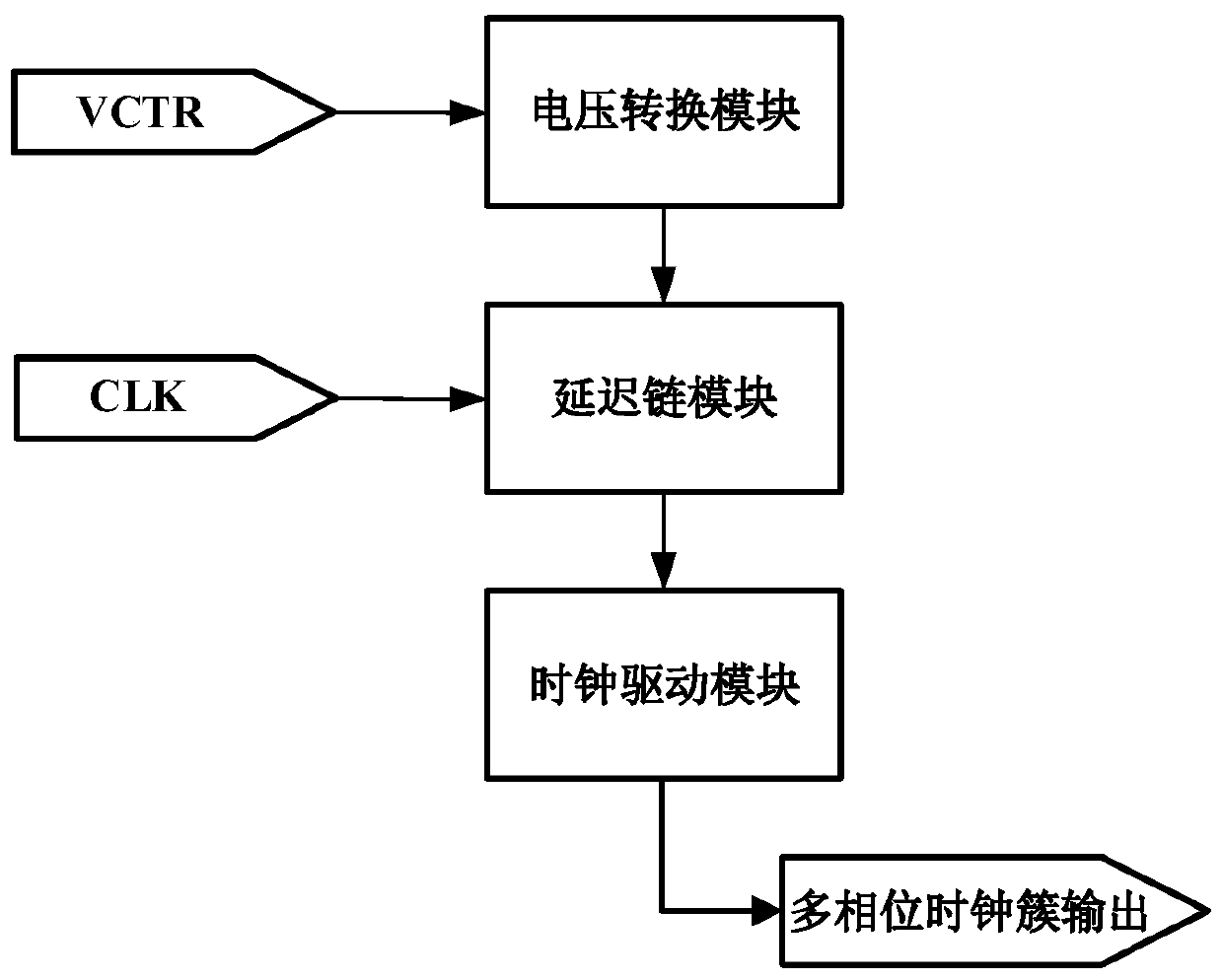
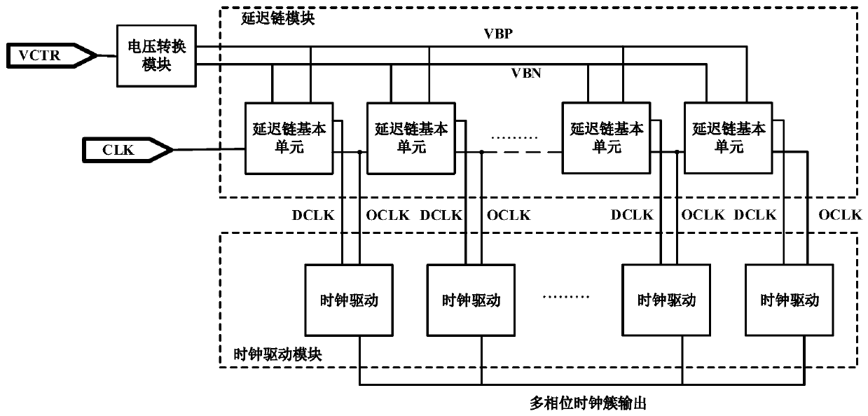
[0050] See figure 1 , figure 1 It is a schematic structural diagram of a clock regeneration delay chain with high precision and low kickback noise provided by an embodiment of the present invention, including:
[0051] A voltage conversion module, connected to the voltage input terminal, for converting the input signal into a first voltage signal and a second voltage signal;
[0052] The delay chain module is connected to the voltage conversion module and the clock input terminal, and is used to control the clock delay time according to the first voltage signal and the second voltage signal to obtain a first clock signal cluster and a second clock signal cluster;
[0053] The clock driving module is connected to the delay chain module and is used to receive and process the first clock signal cluster and the second clock signal cluster, and output a multi-phase clock signal cluster.
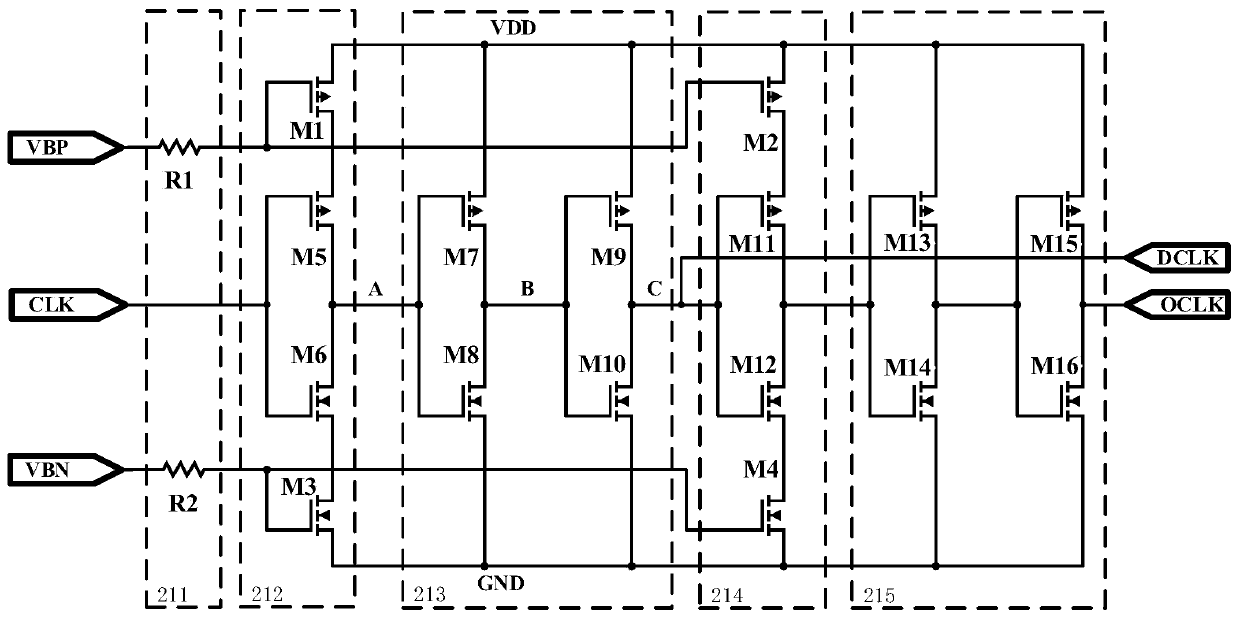
[0054] In this embodiment, the voltage input signal VCTR is connected to the input terminal of the voltage conversion module as a control signal for the delay time of the entire delay chain. The voltage conversion module converts the VCTR signal into a control signal VBP and a control signal VBN, that is, the first voltage The signal and the second voltage signal are output to the delay chain module to control the specific delay time of the delay chain module.
[0055] See figure 2 , figure 2 It is a schematic structural diagram of another clock regeneration delay chain with high precision and low kickback noise provided by an embodiment of the present invention.
[0056] In this embodiment, the delay chain module includes N cascaded delay chain basic units, and the delay chain basic units are all connected to the voltage conversion module; where N is a positive integer. The control signals VBP and VBN are used as input signals, connected to each basic unit of the delay chain, as the specific delay time control signal of the basic unit of the delay chain, the basic unit of the delay chain outputs N DCLK signals and N OCLK signals, that is, the first clock The signal cluster and the second clock signal cluster. The CLK signal is used as an input signal and is connected to the first delay chain basic unit. The output signal of the basic unit of the delay chain is connected to the clock driving module. Correspondingly, the clock driving module includes N clock driving units, and the N clock driving units shown are sequentially connected to the N delay chain basic units.
[0057] In this embodiment, the OCLK signal of the basic unit of the first delay chain is used as the output signal and is connected to the second delay unit and the first clock driving module; the DCLK signal of the basic unit of the first delay chain is also used as the output signal and is connected to the A clock drive module.
[0058] By analogy, the OCLK signal of the basic unit of the N-1th delay chain is used as the output signal, which is connected to the Nth delay unit and the N-1th clock driver module; the DCLK signal of the basic unit of the N-1th delay chain is also used as the output signal , Connected to the N-1th clock drive module.
[0059] The OCLK signal of the basic unit of the Nth delay chain is used as an output signal and connected to the Nth clock driving module; the DCLK signal of the basic unit of the Nth delay chain is also used as an output signal and connected to the Nth clock driving module.
[0060] Finally, the output signals of the first to Nth clock driving modules are N-phase clock signal clusters.
[0061] See image 3 , image 3 It is a schematic diagram of the basic unit structure of a delay chain provided by an embodiment of the present invention. The basic unit of the delay chain includes a low-pass filter subunit 211, a first delay subunit 212, a first clock regeneration subunit 213, and a second delay subunit connected in series in sequence. The unit 214 and the second clock regeneration sub-unit 215.
[0062] In this embodiment, the low-pass filter subunit 211 includes a first resistor R1 and a second resistor R2; wherein one end of the first resistor R1 is connected to the voltage conversion module, and the other end is connected to the first delay Subunit 212 and the second delay subunit 214;
[0063] One end of the second resistor R2 is connected to the voltage conversion module, and the other end is connected to the first delay sub-unit 212 and the second delay sub-unit 214.
[0064] In this embodiment, the first delay subunit 212 includes transistors M1, M5, M6, and M3 connected in series to the power terminal VDD and GND in sequence; wherein, the transistors M1, M5 are PMOS transistors, and the transistor M6 , M3 is NMOS tube;
[0065] The source of the transistor M1 is connected to the power supply VDD terminal, and the source of the transistor M3 is connected to the GND terminal;
[0066] The gate of the transistor M1 is connected to the voltage conversion module through the first resistor R1;
[0067] The gate of the transistor M3 is connected to the voltage conversion module through the second resistor R2;
[0068] The gates of the transistors M5 and M6 are connected to each other and connected to the clock input terminal.
[0069] In this embodiment, the first delay subunit mainly plays the role of delay. The principle is that M3 and M1 are used as current sources to control the image 3 The maximum current of the charge and discharge of the middle node A, thereby delaying the rising (falling) speed of the rising edge (falling edge) of the A node signal, thereby playing the role of delay.
[0070] The traditional voltage-controlled delay chain is controlled by the voltage-controlled line to control the charge and discharge current of the MOS tube. The gate source, gate drain, and gate lining capacitance of the MOS tube have paths for high-frequency signals, and for large swing signals such as clock signals, it is very easy to cause the capacitive coupling to generate kickback noise, which affects voltage control. Voltage, this phenomenon is especially obvious when multiple delay units are cascaded and multiple delay chains are connected. In addition, due to the long length of the delay line, it is very likely to pass, cross, and bypass multiple other circuit modules in actual production, so it is extremely susceptible to noise generated by other modules.
[0071] In this embodiment, the low-pass filter introduced between the noise source and the voltage control line reduces the influence of the high-frequency clock signal on the voltage control line and ensures the consistency of the generated multi-phase clock phase intervals.
[0072] See Figure 4 , Figure 4 Is the equivalent circuit diagram of the low-pass filter provided by the embodiment of the present invention; in the figure, R out Represents the output impedance of the voltage controlled MOS tube, C gs Represents the gate capacitance of the voltage-controlled MOS tube, C represents the output capacitance of the voltage conversion module, R load Represents the output resistance, R represents the introduced filter resistance, when the resistance is not introduced, the noise current I generated by the noise current source noise The voltage response generated on the voltage control line can be expressed as:
[0073]
[0074] When the low-pass filter capacitor is introduced, the voltage response of the noise current generated by the noise current source on the voltage control line can be expressed as:
[0075]
[0076] Considering the actual parameters of the two voltage response expressions and comparing them, it can be obtained that the introduced low-pass filter reduces the high-frequency noise response by approximately (sCgsR+1) times.
[0077] In this embodiment, the first clock regeneration subunit 213 includes transistors M7, M8, M9, and M10; wherein, the transistors M7 and M9 are PMOS tubes, and the transistors M8 and M10 are NMOS tubes;
[0078] The gate of the transistor M7 is connected to the common drain terminal of the transistors M5 and M6, and the source of the transistor M7 is connected to the power supply VDD terminal;
[0079] The gate of the transistor M8 is connected to the gate of the transistor M7 and connected to the common drain of the transistors M5 and M6, the source of the transistor M8 is connected to the GND terminal, and the drain of the transistor M8 is connected to the The drain of the transistor M7;
[0080] The gate of the transistor M9 is connected to the common drain terminal of the transistors M7 and M8, and the source of the transistor M9 is connected to the power supply VDD terminal;
[0081] The gate of the transistor M10 is connected to the gate of the transistor M9 and connected to the common drain terminal of the transistors M7 and M8, the source of the transistor M10 is connected to the GND terminal, and the drain of the transistor M10 is connected to the The drain of the transistor M9 is also used as the output terminal of the first clock regeneration subunit to output the first clock signal, that is, the DCLK signal.
[0082] In this embodiment, the N first clock signals output by the N cascaded delay chain basic units are the first clock signal clusters.
[0083] In the traditional delay chain, the basic delay unit is mainly constructed by the delay module. After the signal passes through this unit, the rising and falling edges of the output will slow down; if the cascade count increases, the final output signal may not reach VDD before the rise , It begins to decrease, which causes the duty cycle to deteriorate; if the cascade count continues to increase, the duty cycle continues to deteriorate, and eventually the signal cannot be effectively reversed, that is, the duty cycle is 0. See Figure 5 , Figure 5 It is a schematic diagram of multi-phase clock pulse contraction output by a basic delay unit built by a delay module according to an embodiment of the present invention.
[0084] In this embodiment, by adding a clock regeneration unit, while adjusting the voltage-controlled delay time, the duty cycle of the clock is restored, so that the output clock of each voltage-controlled delay unit has a certain clock delay and has steep rising and falling edges. Thereby ensuring the consistency of the duty cycle of the multi-phase clock.
[0085] The clock regeneration unit only records the delay time by charging and discharging an unlimited inverter group, recovering the clock rising and falling speed. Take the rising edge of the input signal CLK as an example, see Image 6 , Image 6 It is a schematic diagram of the signal waveform of the CLK signal after being delayed by the basic delay unit provided by the embodiment of the present invention; after the CLK signal is delayed and inverted by the first delay subunit, image 3 The middle A point becomes the falling edge, the discharge current of the A point signal is limited, so the falling edge of the A point signal is delayed; thereby achieving the purpose of delay. After the first clock regeneration subunit, since the charge and discharge current is not controlled by the current source, the signal waveforms of the B node and the C node can be established most quickly, and the clock duty cycle can be recovered.
[0086] In this embodiment, the second delay subunit 214 includes transistors M2, M11, M12, and M4 serially connected to the power supply terminal VDD and GND in sequence; wherein the transistors M2, M11 are PMOS transistors, and the transistors M12, M4 NMOS tube;
[0087] The source of the transistor M2 is connected to the power supply VDD terminal, and the source of the transistor M4 is connected to the GND terminal;
[0088] The gate of the transistor M2 is connected to the voltage conversion module through the first resistor R1;
[0089] The gate of the transistor M4 is connected to the voltage conversion module through the second resistor R2;
[0090] The gates of the transistors M11 and M12 are connected to each other and connected to the output terminal of the first clock regeneration subunit.
[0091] The second clock regeneration subunit 215 includes transistors M13, M14, M15, and M16; wherein, the transistors M13 and M15 are PMOS tubes, and the transistors M14 and M16 are NMOS tubes;
[0092] The gate of the transistor M13 is connected to the common drain terminal of the transistors M11 and M12, and the source of the transistor M13 is connected to the power supply VDD terminal;
[0093] The gate of the transistor M14 is connected to the gate of the transistor M13 and to the common drain of the transistors M11 and M12, the source of the transistor M14 is connected to the GND terminal, and the drain of the transistor M14 is connected to the The drain of the transistor M13;
[0094] The gate of the transistor M15 is connected to the common drain terminal of the transistors M13 and M14, and the source of the transistor M15 is connected to the power supply VDD terminal;
[0095] The gate of the transistor M16 is connected to the gate of the transistor M15 and connected to the common drain of the transistors M13 and M14, the source of the transistor M16 is connected to the GND terminal, and the drain of the transistor M16 is connected to the The drain of the transistor M15 is also used as the output terminal of the second clock regeneration subunit to output the second clock signal, that is, the OCLK signal.
[0096] In this embodiment, the N second clock signals output by the N cascaded delay chain basic units are the second clock signal clusters.
[0097] The working principles of the second delay subunit and the second clock regeneration subunit are the same as those of the first delay subunit and the first clock regeneration subunit, and will not be repeated here.
[0098] See Figure 7 , Figure 7 It is a comparison diagram of the traditional delay chain provided by the embodiment of the present invention and the delay effect of the present invention. In this embodiment, due to the inherent delay of the introduced clock regeneration unit, the inherent delay of the delay chain unit is increased, so that the voltage control line adjustment range can be correspondingly reduced to reach the same delay time, which makes the voltage control delay slow The accuracy is effectively improved, and the anti-noise performance of the voltage-controlled delay chain is improved, which ensures that the voltage-controlled voltage change required for the same delay time difference increases, so it is more suitable for high-precision, multi-chain delay chain phase-locked loops and their components. Time digital detection system.