PCB solder resist detection and repair all-in-one machine and technology method

An all-in-one machine and PCB board technology, applied in measuring devices, printed circuit maintenance/calibration, instruments, etc., can solve the problems of complex repair aids and preparation work, low efficiency, uncertain factors in identification or reading, etc., to achieve saving The effects of repairing aids and preparations, improving accuracy, and saving manpower and equipment costs

Active Publication Date: 2020-01-10
선전진신테크놀로지컴퍼니리미티드
View PDF5 Cites 8 Cited by
  • Summary
  • Abstract
  • Description
  • Claims
  • Application Information

AI Technical Summary

Problems solved by technology

During the production process of the solder mask of the circuit board, the board surface needs to be inspected and repaired to ensure the control of defective products, such as figure 1 As shown, the currently commonly used detection methods are manual visual inspection at the back end of the solder mask or automatic optical inspection equipment (AOI) for detection and defective product sorting, followed by manual repair or silk screen overprint repair, manual identification of defects or There are uncertain factors in reading, and there is also a dependence on the skills of the restoration personnel. The restoration aids and preparation work involved are complicated and inefficient

Method used


Image

  • PCB solder resist detection and repair all-in-one machine and technology method
  • PCB solder resist detection and repair all-in-one machine and technology method
  • PCB solder resist detection and repair all-in-one machine and technology method

Examples


Embodiment Construction

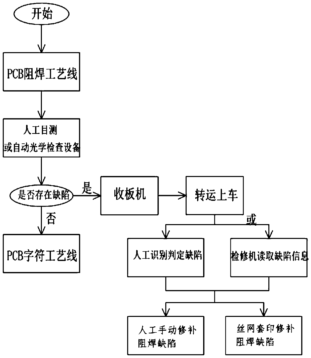
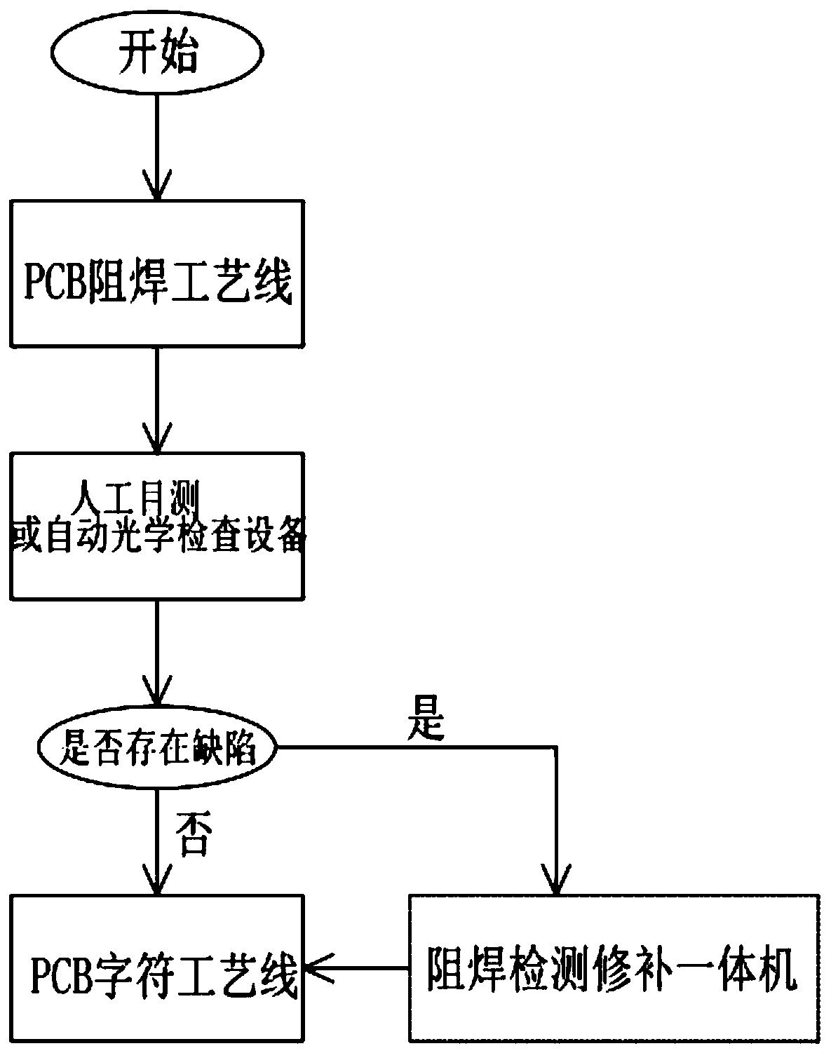
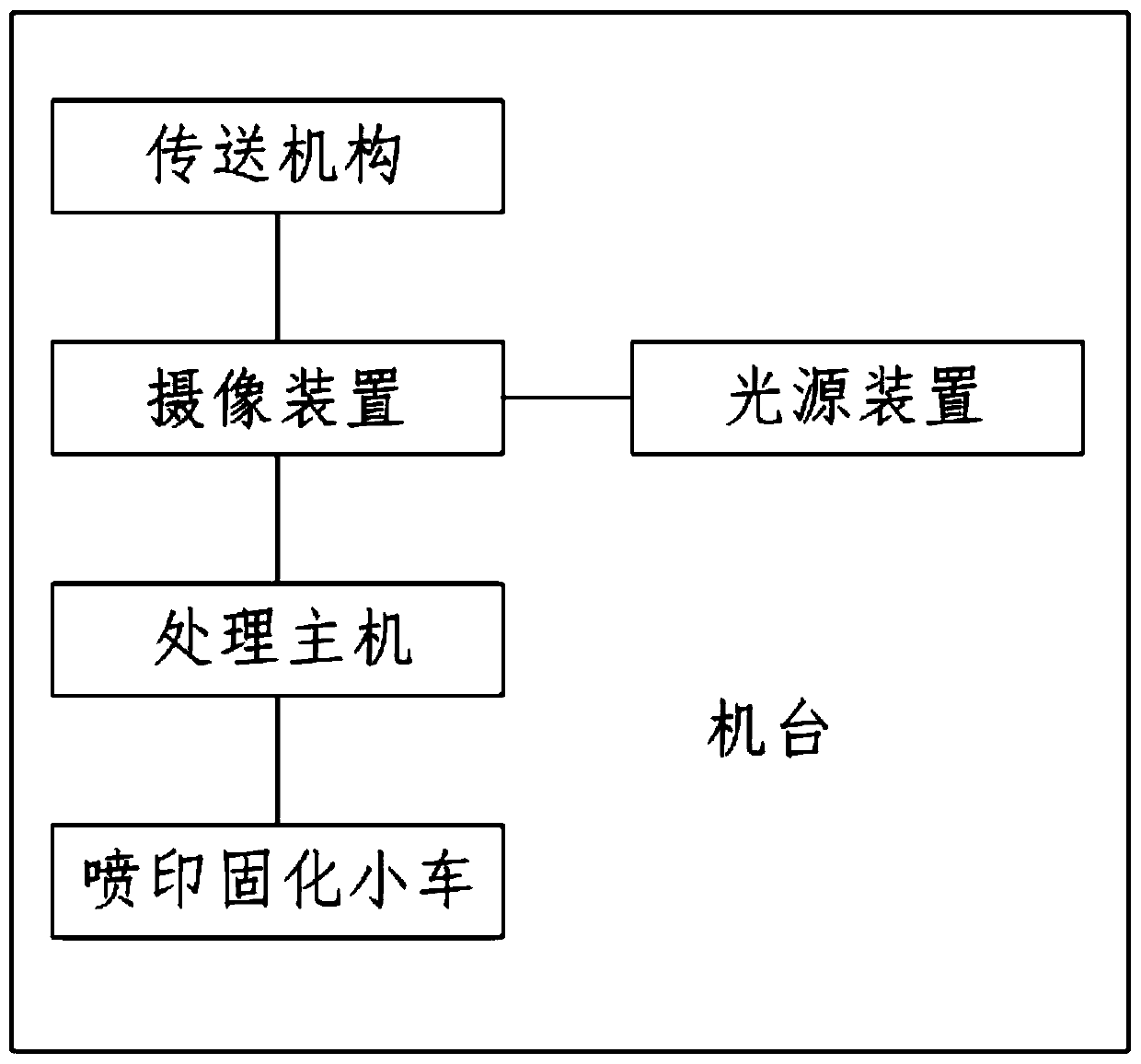
[0027] In order to make the object, technical solution and advantages of the present invention clearer, the present invention will be further described in detail below in conjunction with the accompanying drawings and implementation examples. It should be understood that the specific embodiments described here are only used to explain the present invention, not to limit the present invention.

[0028] It should be noted that all directional indications (such as up, down, left, right, front, back, ...) in the embodiments of the present invention are limited to relative positions on the specified view, rather than absolute positions.

[0029] In addition, in the present invention, descriptions such as "first", "second" and so on are used for description purposes only, and should not be understood as indicating or implying their relative importance or implicitly indicating the quantity of indicated technical features. Thus, the features defined as "first" and "second" may explici...


PUM


Abstract

The invention relates to the printed circuit board manufacturing technology field and especially relates to a PCB solder resist detection and repair all-in-one machine and a technology method. A camera device is used for scanning and photographing a surface of a PCB to obtain an identifiable pattern. An automatic optical detection device is used for automatically identifying and judging defects ofthe PCB, determining defect positions and outputting solder resist defect patterns corresponding to the defect positions. And specific defect area identification, extraction and integration can be performed in time according to the solder resist defect patterns, a corresponding defect repair pattern of the whole PCB is generated, and a piezoelectric ceramic jet printing and curing device adopts apiezoelectric ceramic jet printing technology to repair a solder resist defect. Compared with the prior art, by using the PCB solder resist detection and repair all-in-one machine and the technologymethod of the invention, uncertainty caused by manual operation is overcome, working accuracy is effectively improved, a production process is shortened, manpower and equipment cost are saved, the solder resist defects caused by various reasons can be repaired, and practical and flexible performance is achieved.

Description

【Technical field】 [0001] The invention relates to the technical field of printed circuit board manufacturing, in particular to a PCB solder resistance detection and repair integrated machine and a process method. 【Background technique】 [0002] The solder mask on the surface of the PCB circuit board is commonly known as green oil because most of it is green. Its function is to prevent short circuits of different degrees caused by moisture and chemicals between conductor lines, and to prevent faults caused by poor operation during the production and assembly of components. Open the circuit to prevent the part of the conductor from being stained with tin. It is also a permanent protective layer of the circuit board, which can prevent moisture, corrosion, mildew and mechanical scratches, etc., so as to ensure the good electrical function of the circuit board. During the production process of the solder mask of the circuit board, the board surface needs to be inspected and repai...

Claims


Application Information

Patent Timeline
Patent Type & Authority Applications(China)
IPC IPC(8): H05K3/22H05K3/28G01N21/956
CPCG01N21/956G01N2021/95638H05K3/225H05K3/282H05K2203/013H05K2203/163
Inventor 徐进刘玲
Owner 선전진신테크놀로지컴퍼니리미티드
Why Eureka
Try Eureka