

Wafer warpage adjustment method and equipment
An adjustment method and technology for adjusting equipment, applied in electrical components, semiconductor/solid-state device manufacturing, circuits, etc., can solve the problem that thin film deposition cannot fully adjust the anisotropic warpage of the wafer surface, and ensure process stability and product quality. Yield effect
- Summary
- Abstract
- Description
- Claims
- Application Information
AI Technical Summary
Problems solved by technology
Method used
Image

Examples
Embodiment 1
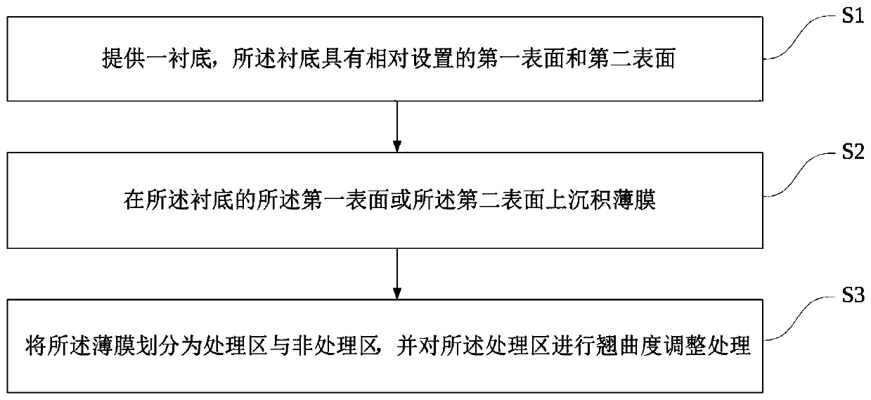
[0071] see Figure 1 to Figure 9 , the present embodiment provides a method for adjusting wafer warpage, characterized in that it includes the following steps:
[0072] 1) providing a wafer, the wafer has a first surface and a second surface oppositely arranged;
[0073] 2) depositing a thin film on the first surface or the second surface of the wafer;
[0074] 3) Dividing the film into a treated area and a non-treated area, and performing warpage adjustment treatment on the treated area.
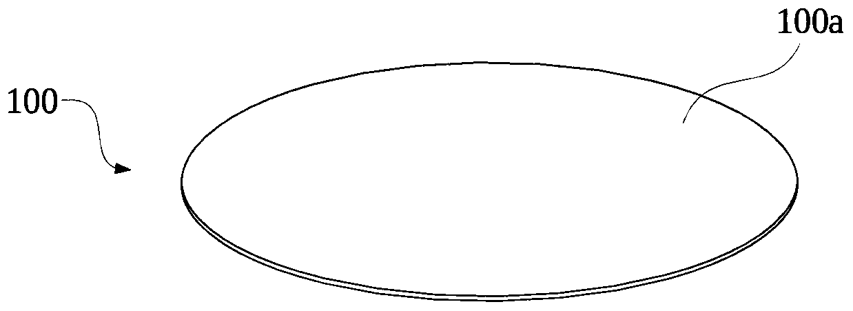
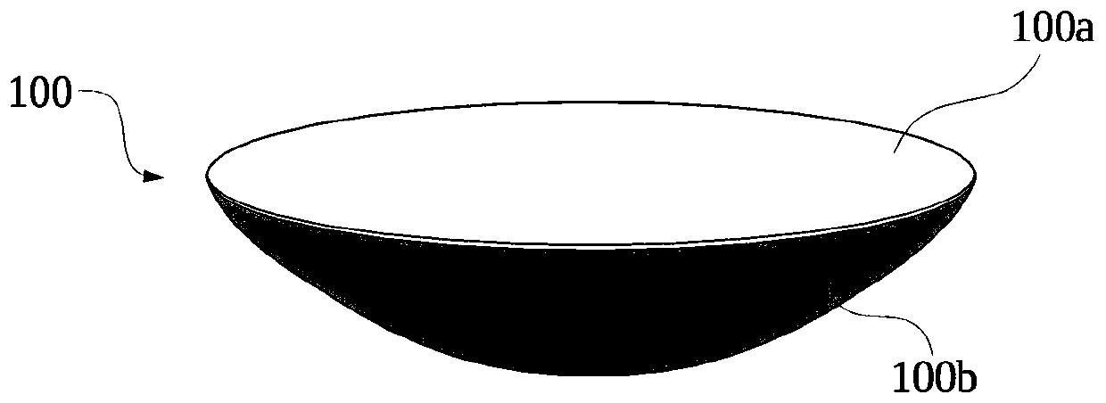
[0075] In step 1), see figure 1 S1 and figure 2 , providing a wafer 100, the wafer 100 has a first surface 100a and a second surface 100b disposed opposite to each other.
[0076] Such as figure 2 As shown, the wafer 100 is normal without warpage. Once the wafer is warped, it may affect the alignment of the patterning process, and even cause fragmentation due to stress. Therefore, in the manufacturing process of semiconductor wafers, it is generally expected to obtain figure 2 Th...
Embodiment 2
[0091] see Figure 10 to Figure 11 , this embodiment provides a wafer warpage adjustment device, characterized in that: comprising:
[0092] A thin film growth module is used to deposit a thin film on the surface of a wafer, the wafer has a first surface and a second surface oppositely arranged, and the thin film growth module is on the first surface or the second surface of the wafer deposition of thin films on the surface;
[0093] The warpage adjustment processing module is used to divide the film into a treatment area and a non-treatment area, and perform warpage adjustment processing on the treatment area.
[0094] Such as Figure 10Shown is a schematic diagram of the thin film growth module 300 provided in this embodiment. The wafer 301 is accommodated in a closed chamber 302 and held by a wafer holding device 303 . The direction in which the silicon nitride film 304 needs to be grown on the back side of the wafer 301 is provided with a plasma generator 305, which ge...
PUM
 Abstract
Description
Claims
Application Information