Laser annealing device

A laser annealing and laser technology, which is applied in the field of lasers, can solve the problems of not being able to maximize the output of lasers, reduce the influence of machine spot, and ensure the stability of the process

Active Publication Date: 2019-07-30
SHANGHAI MICRO ELECTRONICS EQUIP (GRP) CO LTD
View PDF5 Cites 3 Cited by
  • Summary
  • Abstract
  • Description
  • Claims
  • Application Information

AI Technical Summary

Problems solved by technology

[0004] The embodiment of the present invention provides a laser annealing device

Method used


Image

  • Laser annealing device
  • Laser annealing device
  • Laser annealing device

Examples


Example Embodiment

[0030] In order to make the objectives, technical solutions and advantages of the present invention clearer, the following will clearly and completely describe the technical solutions of the present invention through implementations with reference to the drawings in the embodiments of the present invention. Obviously, the described embodiments are the present invention. Some embodiments, not all embodiments. Based on the embodiments of the present invention, all other embodiments obtained by those of ordinary skill in the art without creative work shall fall within the protection scope of the present invention.
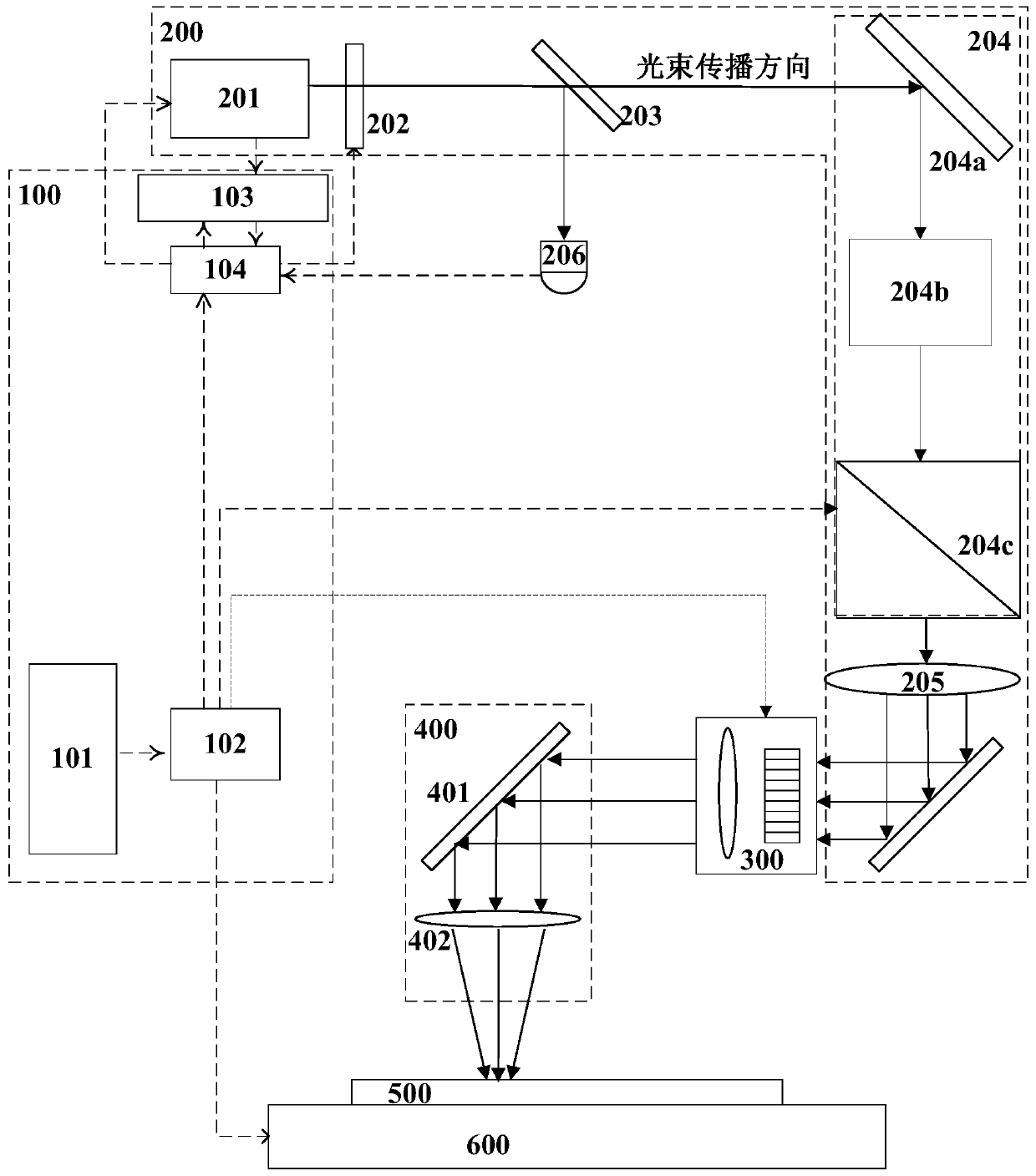
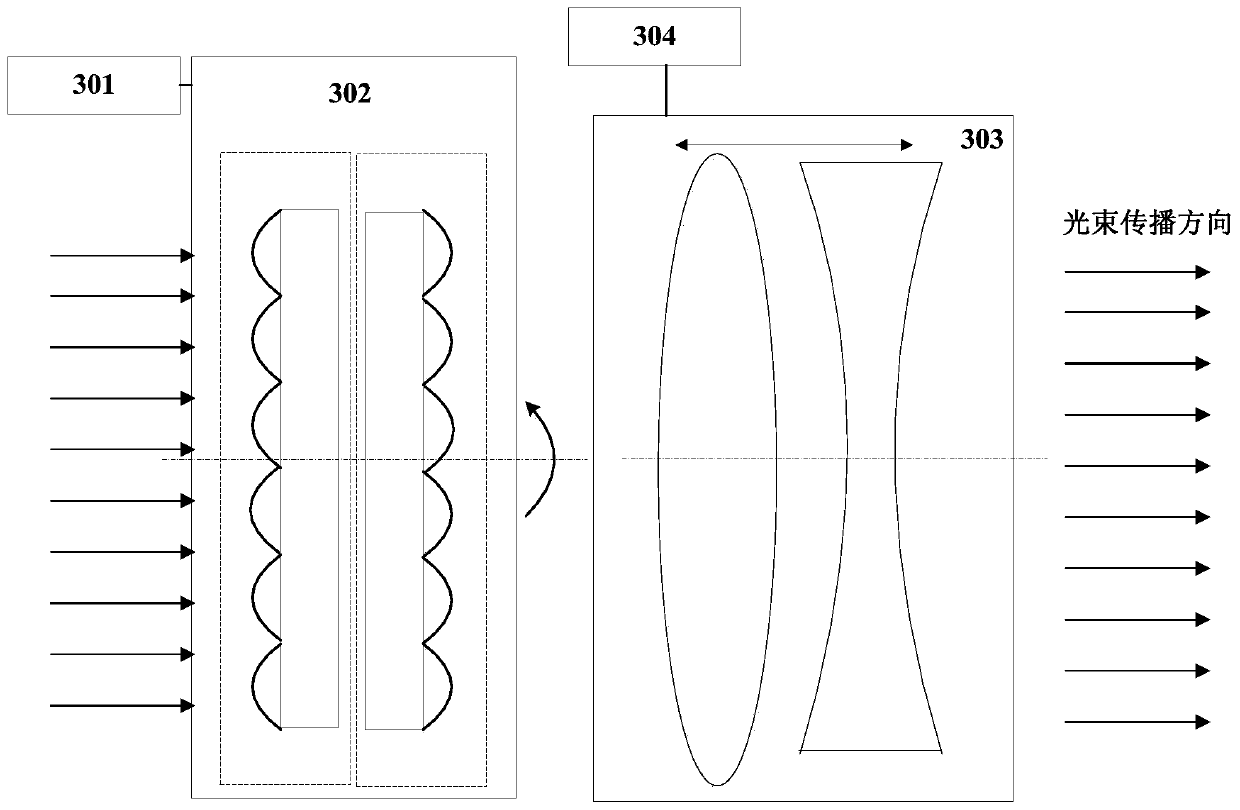
[0031] reference figure 1 Shown is a schematic diagram of a laser annealing device provided by an embodiment of the present invention. The laser annealing device can be directly applied to semiconductor surface annealing, and can also be applied to the fields of glass substrate, metal material surface heat treatment, etc., especially according to actual needs. Adjust the...


PUM


Abstract

The embodiment of the invention discloses a laser annealing device which comprises a control module, a laser beam generation module, a laser beam adjustment module and an optical module. The laser beam generation module is electrically connected with the control module and is used for producing a first laser beam according to a laser control signal output by the control module; the laser beam adjustment module is electrically connected with the control module and is used for adjusting the laser intensity distribution of the first laser beam so as to convert into a second laser beam according to a movable mechanism parameter output by the control module; and the optical module is used for converging the second laser beam so as to form a light spot corresponding to the laser control signal on a correspondingly arranged substrate. According to the laser annealing device provided by the embodiment of the invention, no matter how the quality of a light beam output by the laser changes, thefirst laser beam cannot be influenced, and uncertain influences cannot bring to the process; and the yield of the laser has no need to be frequently adjusted, so that the maximum utilization of the yield of the laser is ensured.

Description

technical field [0001] Embodiments of the present invention relate to laser technology, and in particular to a laser annealing device. Background technique [0002] Annealing mainly refers to the heat treatment process in which the material is exposed to high temperature for a long time and then cooled slowly. Traditional furnace heating annealing, even at temperatures as high as 1100 degrees, still cannot completely eliminate crystal defects. Laser annealing can eliminate crystal defects more thoroughly. [0003] Existing laser annealing technology, when the silicon wafer requires high-energy exposure, generates a small-sized spot by actively increasing the laser light intensity to achieve strong energy; when the silicon wafer requires low-energy exposure, it actively reduces the laser light intensity. A large spot size is generated to achieve weak energy, and the size of the small spot size and the large spot size are fixed. However, the productivity of the laser is rel...

Claims


Application Information

Patent Timeline
IPC IPC(8): B23K26/00B23K26/06C03B25/00C21D1/26C21D1/34C21D11/00H01L21/268
CPCB23K26/00B23K26/06C03B25/00C21D1/26C21D1/34C21D11/00H01L21/268Y02P40/57
Inventor 周伟许凯迪苏海业黄元昊罗闻
Owner SHANGHAI MICRO ELECTRONICS EQUIP (GRP) CO LTD
Why Eureka
Try Eureka