Preparation method of array sensor of bridging type micro-nano structure sensing unit and product

An array sensor, micro-nano structure technology, applied in the direction of material electrochemical variables, etc., to achieve the effect of improving crystallinity, high sensitivity, and good bridging

Active Publication Date: 2020-01-17
HUAZHONG UNIV OF SCI & TECH
View PDF9 Cites 1 Cited by
  • Summary
  • Abstract
  • Description
  • Claims
  • Application Information

AI Technical Summary

Problems solved by technology

At present, the preparation of arrayed sensors is still in the development stage, and the simple preparation method of arrayed sensors with micro-nano structural units needs to be further improved and developed.

Method used


Image

  • Preparation method of array sensor of bridging type micro-nano structure sensing unit and product
  • Preparation method of array sensor of bridging type micro-nano structure sensing unit and product
  • Preparation method of array sensor of bridging type micro-nano structure sensing unit and product

Examples


preparation example Construction

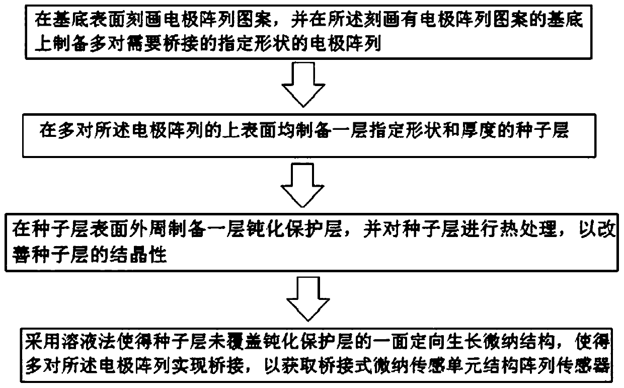
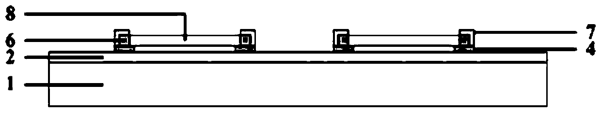
[0038] like figure 1 and figure 2 As shown, the present invention provides a method for preparing an array sensor of a bridged micro-nano structure sensing unit, which specifically includes the following steps:

[0039] S1 Writing an electrode array pattern on the surface of the substrate, and preparing multiple pairs of electrode arrays 4 of a specified shape that need to be bridged on the substrate with the electrode array pattern drawn.

[0040] Specifically, the electrode array pattern is prepared on the surface of the substrate by photolithography, and the electrode array 4 is prepared on the surface of the substrate by deposition and solution stripping. However, in the present invention, it is not limited to photolithography, deposition and solution stripping. Any technical means and method that can realize the preparation of multiple pairs of electrode arrays 4 of a specified shape that need to be bridged on the substrate in this solution can be used. Furthermore, in...

Embodiment 1

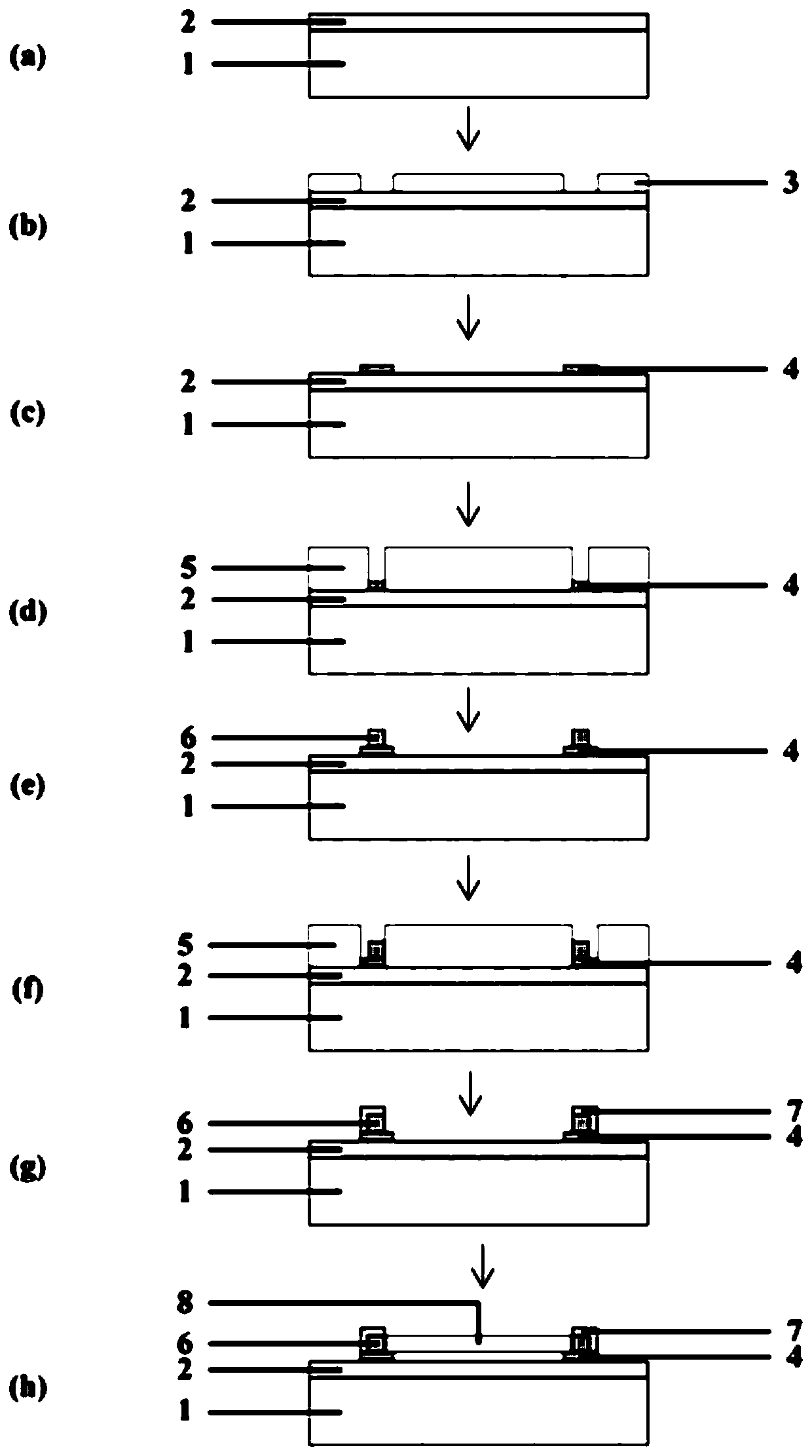
[0060] S1 uses AZ5214 photoresist as a thin glue to prepare a square-based electrode array pattern on the surface of the substrate;

[0061] S2 uses magnetron sputtering to prepare an Au electrode array on the surface of the substrate and uses a degumming solution to peel off the metal electrodes;

[0062] S3 uses overlay technology to prepare the seed layer pattern of the micro-nano structure sensing unit on the surface of the substrate and the electrode, that is, the pattern of the bridge pier, and the shape is square;

[0063] S4 Prepare the seed layer ZnO of the micro-nano structure sensing unit on the surface of the substrate by means of electron beam evaporation, and perform stripping by solution method, remove the photoresist, and obtain the seed layer ZnO of the micro-nano structure sensing unit on the electrode;

[0064] S5 uses NR21-20000P as a thick glue to carry out photolithography to prepare a passivation protective layer pattern on the seed layer of the electrod...

Embodiment 2

[0070] S1 uses HTI751 photoresist as a thin glue to prepare a rectangular-based electrode array pattern on the surface of the substrate;

[0071] S2 uses thermal evaporation to prepare an Ag electrode array on the surface of the substrate and uses a degumming solution to peel off the metal electrodes;

[0072] S3 uses overlay technology to prepare the seed layer pattern of the micro-nano structure sensing unit on the surface of the substrate and the electrode, that is, the pattern of the bridge pier, and the shape is rectangular;

[0073] S4 Prepare the seed layer Cu of the micro-nano structure sensing unit on the surface of the substrate by magnetron sputtering, and perform stripping by solution method, remove the photoresist, and obtain the seed layer Cu of the micro-nano structure sensing unit on the electrode;

[0074] S5 uses NR26-25000P as a thick glue for photolithography to prepare a passivation protective layer pattern on the seed layer of the electrode and micro-nano...


PUM

PropertyMeasurementUnit
thicknessaaaaaaaaaa
thicknessaaaaaaaaaa

Abstract

The invention belongs to the field of micro-nano sensor preparation, and particularly discloses a preparation method of an array sensor of a bridging type micro-nano structure sensing unit and a product. The method comprises the following steps: preparing a plurality of pairs of electrode arrays in a specified shape needing to be bridged on the surface of a substrate, then preparing a seed layer with a specified shape and thickness, then preparing a passivation protection layer on the periphery of the surface of the seed layer except the bridging surface, carrying out heat treatment on the seed layer to improve the crystallinity of the seed layer, and finally growing a micro-nano structure in a directional mode by adopting a solution method, so that the plurality of pairs of electrode arrays are bridged. The product comprises a substrate, an electrode array, a seed layer, a passivation protection layer and a micro-nano structure, and the micro-nano structure grows on one surface, not covered with the passivation protection layer, of the seed layer, so that the bridging of the pair of electrode arrays is realized. The sensor prepared by the invention has the characteristics of highsensitivity and high fault tolerance, and the junction resistance between sensitive layers of a traditional bridging type micro-nano structure sensor is greatly reduced.

Description

technical field [0001] The invention belongs to the field of preparation of micro-nano sensors, and more specifically relates to a preparation method and product of an array sensor of a bridge-type micro-nano structure sensing unit. Background technique [0002] Due to the size effect, micro-nano materials have physical and chemical properties that traditional materials do not have, such as: (1) special optical, thermal, magnetic and mechanical properties; (2) surface effects; (3) quantum size effects; (4) Macroscopic quantum tunneling effect; (5) Dielectric confinement effect. The unique effect makes it show its talents in the field of sensing, showing more advantageous performance than traditional materials. The huge specific surface area of ​​micro-nano materials enables micro-nano materials to improve performance such as sensitivity and response speed by tens of times or even several orders of magnitude. However, nanosensors, especially nanosensor arrays, cannot be wid...

Claims


Application Information

Patent Timeline
Patent Type & Authority Applications(China)
IPC IPC(8): G01N27/30
CPCG01N27/30
Inventor 史铁林林建斌廖广兰方涵韩航迪
Owner HUAZHONG UNIV OF SCI & TECH
Why Eureka
Try Eureka