
Optical laminate
A technology of optical laminates and absorbing layers, applied in optics, optical components, nonlinear optics, etc., can solve problems such as abnormal hue, high cost, and reduced brightness, and achieve sufficient brightness, suppress reflectivity, and achieve cost-effective effects
- Summary
- Abstract
- Description
- Claims
- Application Information
AI Technical Summary
Problems solved by technology
Method used
Image

Examples
Embodiment 1
[0147] (wavelength conversion layer)
[0148] A commercially available TV (manufactured by Samsung, trade name "UN65JS9000FXZA") was disassembled to obtain a quantum dot sheet which is a wavelength conversion material contained on the backlight side. This quantum dot sheet is used as the wavelength conversion layer (1).
[0149] (absorbent layer)
[0150] Contains 0.3 wt. Parts, 1 part by weight of isocyanate crosslinking agent (manufactured by Tosoh, trade name "Coronate L"), 0.3 parts by weight of pigment (manufactured by Yamada Chemical Industry Co., Ltd., trade name "FDG-007"), phenolic antioxidant ( BASF Japan company make, brand name "IRGANOX1010") 0.2 weight part, and the pigment-containing adhesive was manufactured. The pigment-containing adhesive obtained above was applied with an applicator to a thickness of 20 μm on a PET substrate (manufactured by Mitsubishi Plastics Corporation, trade name "MRF38CK") subjected to a treatment to make the adhesive easy to peel, a...
Embodiment 2
[0154] (absorbent layer)
[0155] 0.3 parts by weight of the pigment used (manufactured by Yamada Chemical Industry Co., Ltd., trade name "FDG-007") was changed to 0.3 parts by weight of pigment (manufactured by Yamada Chemical Industry Co., Ltd., trade name "FDG-004"). Otherwise, the absorbing layer (2) was formed on TAC in the same manner as in Example 1. In addition, the dye used (manufactured by Yamada Chemical Industry Co., Ltd., trade name "FDG-004") is a compound having an absorption peak at a wavelength of 600 nm.
[0156] (optical laminate)
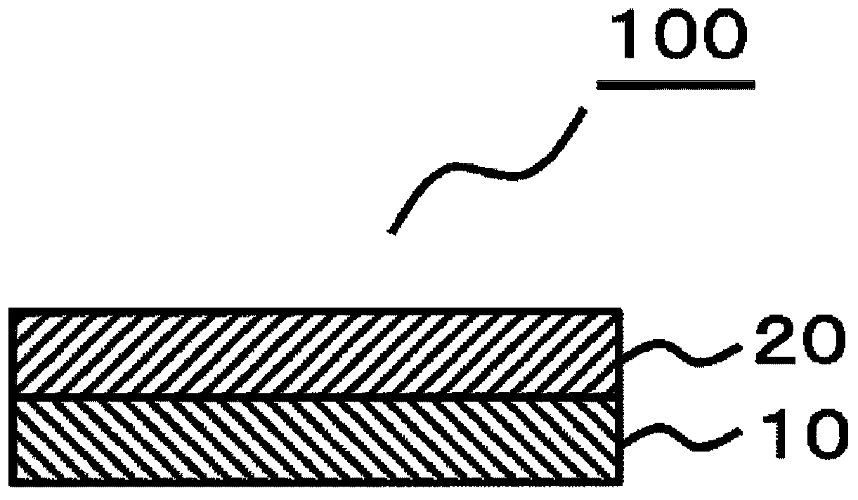
[0157] The wavelength conversion layer (1) obtained in Example 1 and the above-mentioned absorption layer (2) were laminated to obtain an optical laminate (2) having a laminated structure of a wavelength conversion layer / absorption layer. The results are shown in Table 1.
Embodiment 3
[0159] (absorbent layer)
[0160] 0.3 parts by weight of the pigment used (manufactured by Yamada Chemical Industry Co., Ltd., trade name "FDG-007") was changed to 0.3 parts by weight of pigment (manufactured by Yamada Chemical Industry Co., Ltd., trade name "FS-1531"). Otherwise, the absorbing layer (3) was formed on TAC in the same manner as in Example 1. In addition, the dye used (manufactured by Yamada Chemical Industry Co., Ltd., trade name "FS-1531") is a compound having an absorption peak at a wavelength of 700 nm.
[0161] (optical laminate)
[0162] The wavelength conversion layer (1) obtained in Example 1 and the above-mentioned absorption layer (3) were laminated to obtain an optical laminate (3) having a laminated structure of a wavelength conversion layer / absorption layer. The results are shown in Table 1.
PUM
| Property | Measurement | Unit |
|---|---|---|
| thickness | aaaaa | aaaaa |
| thickness | aaaaa | aaaaa |
| thickness | aaaaa | aaaaa |
Abstract
Description
Claims
Application Information