
Sheet material, metal mesh, wiring substrate, display device and manufacturing methods therefor

A wiring substrate and manufacturing method technology, applied in identification devices, printed circuit manufacturing, metal layered products, etc., can solve problems such as invisibility, and achieve the effects of large viewing angle, high adhesion, and long life

Active Publication Date: 2019-02-05
TDK CORPARATION
View PDF7 Cites 0 Cited by
  • Summary
  • Abstract
  • Description
  • Claims
  • Application Information

AI Technical Summary

Problems solved by technology

[0003] Compared with conventional transparent conductive films such as ITO (Indium Tin Oxide), the metal mesh is superior in that it can achieve cost reduction and low resistance. In the case of use, sometimes invisibility becomes a problem compared to ITO

Method used


Image

  • Sheet material, metal mesh, wiring substrate, display device and manufacturing methods therefor
  • Sheet material, metal mesh, wiring substrate, display device and manufacturing methods therefor
  • Sheet material, metal mesh, wiring substrate, display device and manufacturing methods therefor

Examples


Embodiment 1

[0123] A resin composition containing 20% ​​by mass of palladium particles and an isocyanate resin was prepared.

[0124] The obtained resin composition was coated on a PET film (manufactured by Toyobo Co., Ltd., trade name: COSMOSHINE A4100) and dried to obtain a resin having palladium particles with a thickness of 60 μm exposed on the surface of the PET film. Layer 1 laminate. The first laminate is immersed in an electroless plating solution tank containing 0.5 g / L nickel ions, and electroless plating is performed for 20 seconds at a temperature of the plating solution tank of 82° C. to obtain a surface with unevenness. The second laminated body in which the first electroless plating film is formed. Next, the second laminate was immersed in an electroless plating solution tank containing 3.0 g / L copper ions, and electroless plating was performed for 45 minutes at a temperature of the plating solution tank of 38° C. to produce The second electroless plating film is formed o...

Embodiment 2

[0126] A sheet was obtained in the same manner as in Example 1 except that the time of immersion in the electroless plating solution tank containing nickel ions was set to 30 seconds.

Embodiment 3

[0128] A sheet was obtained in the same manner as in Example 1 except that the time of immersion in the electroless plating solution tank containing nickel ions was set to 40 seconds.


PUM

PropertyMeasurementUnit
Thicknessaaaaaaaaaa

Abstract

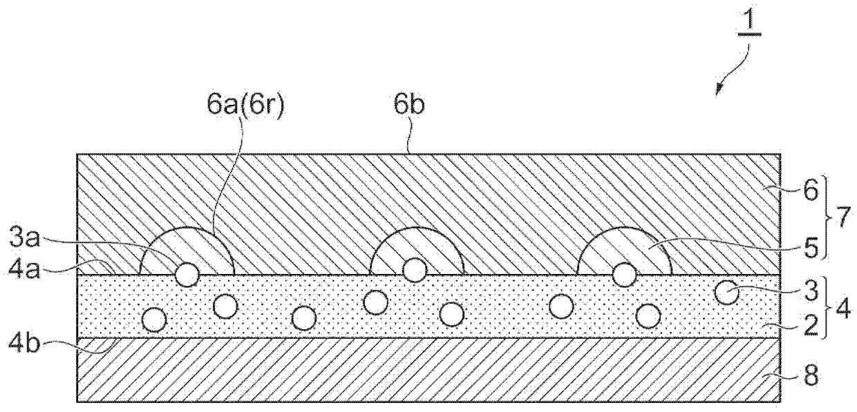
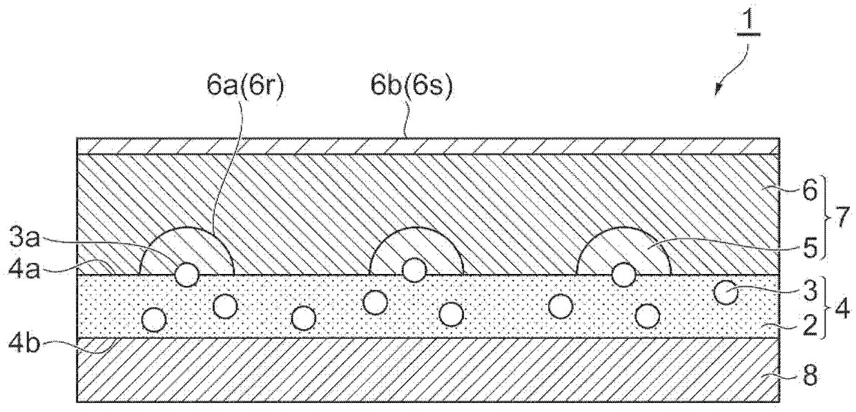
The invention relates to a sheet material (1) provided with: a resin layer (4) including a binder (2) and a catalyst particle (3); a non-electrolytic plated film (7) provided on one main surface (4a)side of the resin layer (4) and having a first electroless plating film (5) and a second electroless plating film (6); and a base material (8) disposed on the other main surface (4b) side of the resinlayer (4). At least a part of the catalyst particles (3) has an exposed surface (3a) exposed from one main surface (4a) of the resin layer (4), and the exposed surface (3a) is dispersed on one main surface (4a) of the resin layer (4). The first electroless plating film (5) is provided on one main surface (4a) of the resin layer (4) so as to surround the exposed surface (3a) of each of the catalyst particles (3). The second electroless plating film (6) is provided so as to cover the first electroless plating film (5), and one main surface (6a) of the second electroless plating film (6) is provided corresponding to the concave (6r) of the first electroless plating film (5).

Description

technical field [0001] The present invention relates to a sheet, a metal mesh, a wiring board, a display device, and a manufacturing method thereof. Background technique [0002] In recent years, attempts have been made to develop metal meshes in which fine wiring of metals such as copper and silver are patterned into a mesh shape as members for electrodes used in electronic components such as touch panels. [0003] Compared with conventional transparent conductive films such as ITO (Indium Tin Oxide), the metal mesh is superior in that it can achieve cost reduction and low resistance. In the case of using it, invisibility sometimes becomes a problem compared with ITO. [0004] As a metal mesh whose invisibility is improved, a metal mesh composed of a copper layer and a blackened metal layer is known. For example, as the blackened metal layer, Patent Documents 1 and 2 disclose a metal mesh using a metal oxide whose corrosion rate is slower than copper, or a metal mesh usin...

Claims


Application Information

Patent Timeline
IPC IPC(8): C23C18/16C23C18/20C23C18/31G09F9/33
CPCC23C18/1641C23C18/165C23C18/1689C23C18/2006C23C18/31G09F9/33H01L23/145H01L23/498H01L25/0753H01L33/62C23C18/161C23C18/1608C23C18/30C23F1/02C23C18/1651C23C18/32C23C18/38B32B27/281B32B2255/205B32B2307/732B32B2307/546B32B2255/26B32B27/36B32B27/38B32B27/06B32B2457/208B32B27/283B32B2307/412B32B2457/202B32B2255/10B32B2255/28H01L2224/16225C23C18/206C23C18/208H05K3/181H05K2201/10106B32B27/08B32B15/09B32B15/20B32B3/30H01L23/52H01L27/156B32B2457/20B32B27/18
Inventor 折笠诚堀川雄平上林义广阿部寿之
Owner TDK CORPARATION
Learn More