Supercharge Your Innovation With Domain-Expert AI Agents!

Semiconductor power element and manufacturing method thereof

A technology of power components and manufacturing methods, which is applied in semiconductor/solid-state device manufacturing, semiconductor devices, electrical components, etc., can solve the problems of increasing the drift area and reducing the collapse voltage of semiconductor power components, and achieve the goal of reducing the on-resistance and reducing the distance Effect

Pending Publication Date: 2020-01-31
SUPER GROUP SEMICON
View PDF6 Cites 0 Cited by
  • Summary
  • Abstract
  • Description
  • Claims
  • Application Information

AI Technical Summary

Problems solved by technology

However, increasing the carrier concentration in the drift region may lead to a decrease in the breakdown voltage of semiconductor power devices

Method used


Image

  • Semiconductor power element and manufacturing method thereof
  • Semiconductor power element and manufacturing method thereof
  • Semiconductor power element and manufacturing method thereof

Examples


Embodiment Construction

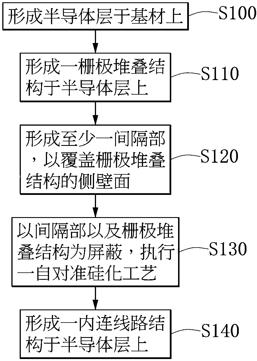
[0037] see figure 1 . figure 1 It is a flowchart of a method for manufacturing a semiconductor power device according to an embodiment of the present invention.

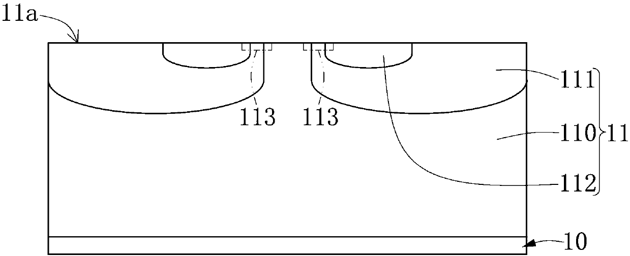
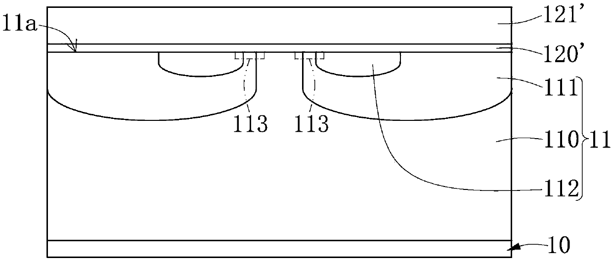
[0038] In step S100, a semiconductor layer is formed on the substrate. Next, in step S110 , a gate stack structure is formed on the semiconductor layer. Subsequently, in step S120 , at least one spacer is formed to cover the sidewall surface of the gate stack structure. In step S130, a self-aligned silicidation process is performed using the spacers and the gate stack structure as a shield. Afterwards, a silicide layer contacting the source region is formed, and in step S140 , an interconnection circuit structure is formed on the semiconductor layer.

[0039] As mentioned above, in this embodiment, before the step of forming the interconnection wiring structure, the spacer covering the sidewall surface of the gate stack structure is firstly formed, and the salicide process is performed. The specific steps in the...


PUM

PropertyMeasurementUnit
thicknessaaaaaaaaaa

Abstract

The invention discloses a semiconductor power element and a manufacturing method thereof. The manufacturing method of the semiconductor power element comprises the steps that a semiconductor layer isformed on a substrate; at least a base region and a source region in the base region are formed in the semiconductor layer, and a channel is defined between the edge of the source region and the edgeof the base region; a gate stack structure is formed on the semiconductor layer and overlaps the channel region in a vertical direction; at least a spaced portion is formed to cover the sidewall surface of the gate stack structure; the spaced portion covers a portion of the source region, and the other part of the source region is exposed on the upper surface; the spaced portion and the gate stackstructure are used as a shield, and a self-aligned silicidation process is performed to form a silicide layer contacting the source region; and an interconnection circuit structure is formed on thesemiconductor layer. The interconnection circuit structure includes at least an interlayer dielectric layer and a source conductive layer electrically connected with the source region. The silicide layer extends from a space below the source conductive layer toward the gate stack structure to a space below the interlayer dielectric layer.

Description

technical field [0001] The invention relates to a semiconductor power element and a manufacturing method thereof, in particular to a vertical double-diffused metal oxide semiconductor field effect transistor and a manufacturing method thereof. Background technique [0002] For existing semiconductor power devices (such as: Horizontal Double-diffused MOSFET (LDMOSFET) and Vertical Double-diffused MOSFET (VDMOSFET)), the breakdown voltage (breakdown voltage) and conduction On-resistance is a more important parameter, wherein the on-resistance will affect the conduction loss (conducting loss, conduction loss) of the semiconductor power element. [0003] Taking the vertical double-diffused transistor as an example, the on-resistance is generally reduced by increasing the carrier concentration in the drift region of the semiconductor power device. However, increasing the carrier concentration in the drift region may lead to a decrease in the breakdown voltage of semiconductor po...

Claims


Application Information

Patent Timeline
Patent Type & Authority Applications(China)
IPC IPC(8): H01L29/78H01L21/336
CPCH01L29/78H01L29/66477H01L29/665
Inventor 唐松年陈和泰许修文
Owner SUPER GROUP SEMICON
Features
  • R&D
  • Intellectual Property
  • Life Sciences
  • Materials
  • Tech Scout
  • Unparalleled Data Quality
  • Higher Quality Content
  • 60% Fewer Hallucinations
Learn More