Method and system for improving PCB inspection precision

A technology for checking accuracy and grammar, applied in the field of optical inspection, can solve the problem of low PCB inspection accuracy, achieve the effect of improving accuracy and accuracy, and improving inspection accuracy

Active Publication Date: 2020-02-04
HUAZHONG UNIV OF SCI & TECH
View PDF6 Cites 2 Cited by
  • Summary
  • Abstract
  • Description
  • Claims
  • Application Information

AI Technical Summary

Problems solved by technology

[0004] In view of the defects of the prior art, the purpose of the present invention is to solve the technical problem that the existing PCB inspection is realized by converting the Gerber file into a bitmap, and the accuracy of the PCB inspection is not high due to the pixel error introduced by the bitmap

Method used


Image

  • Method and system for improving PCB inspection precision
  • Method and system for improving PCB inspection precision
  • Method and system for improving PCB inspection precision

Examples


Embodiment Construction

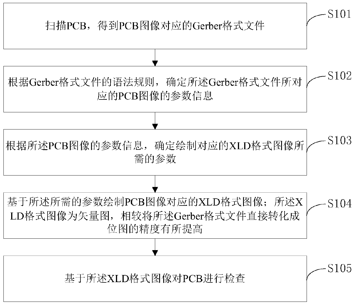
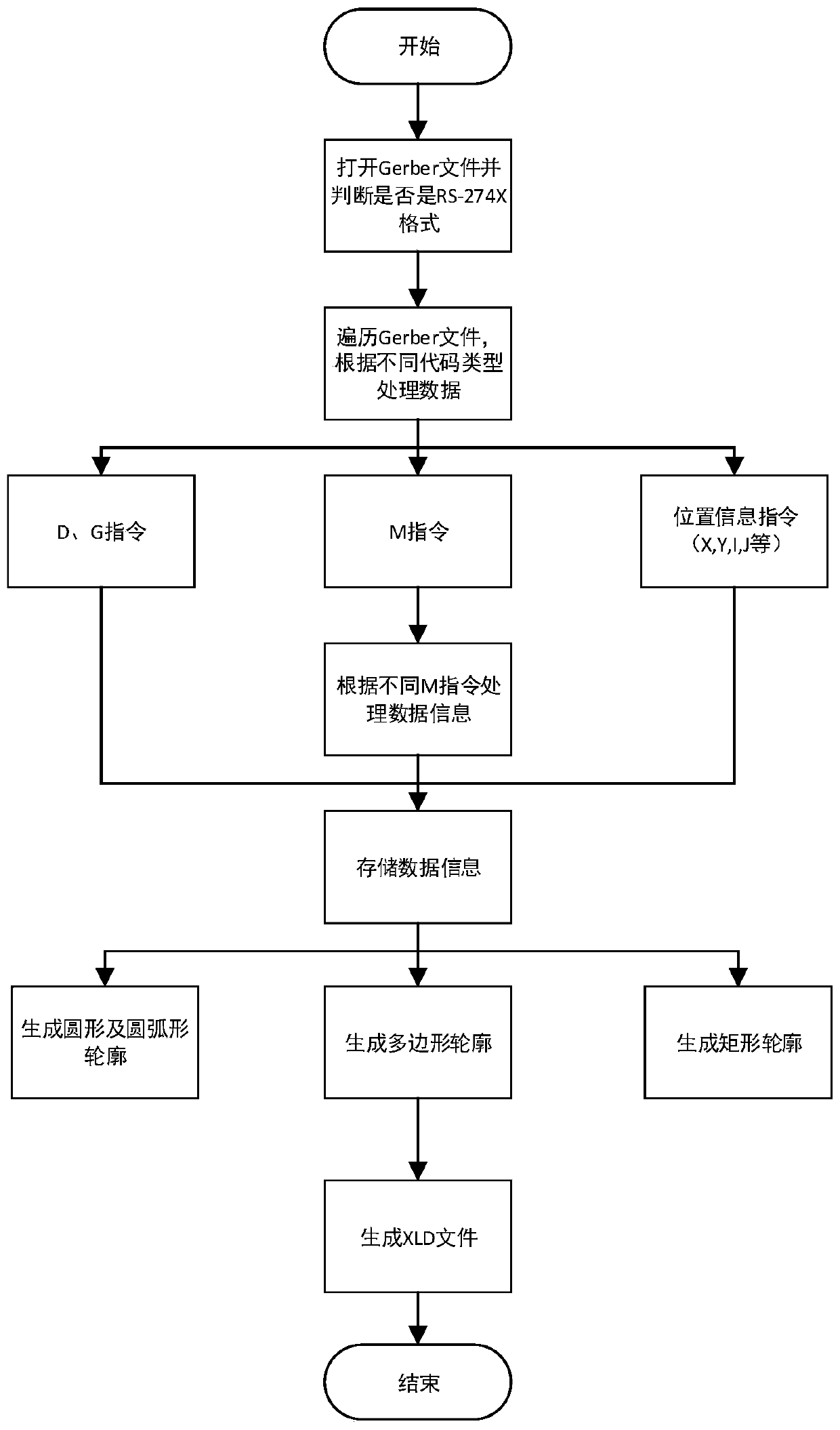
[0036] In order to make the object, technical solution and advantages of the present invention clearer, the present invention will be further described in detail below in conjunction with the accompanying drawings and embodiments. It should be understood that the specific embodiments described here are only used to explain the present invention, not to limit the present invention. In addition, the technical features involved in the various embodiments of the present invention described below may be combined with each other as long as they do not constitute a conflict with each other.

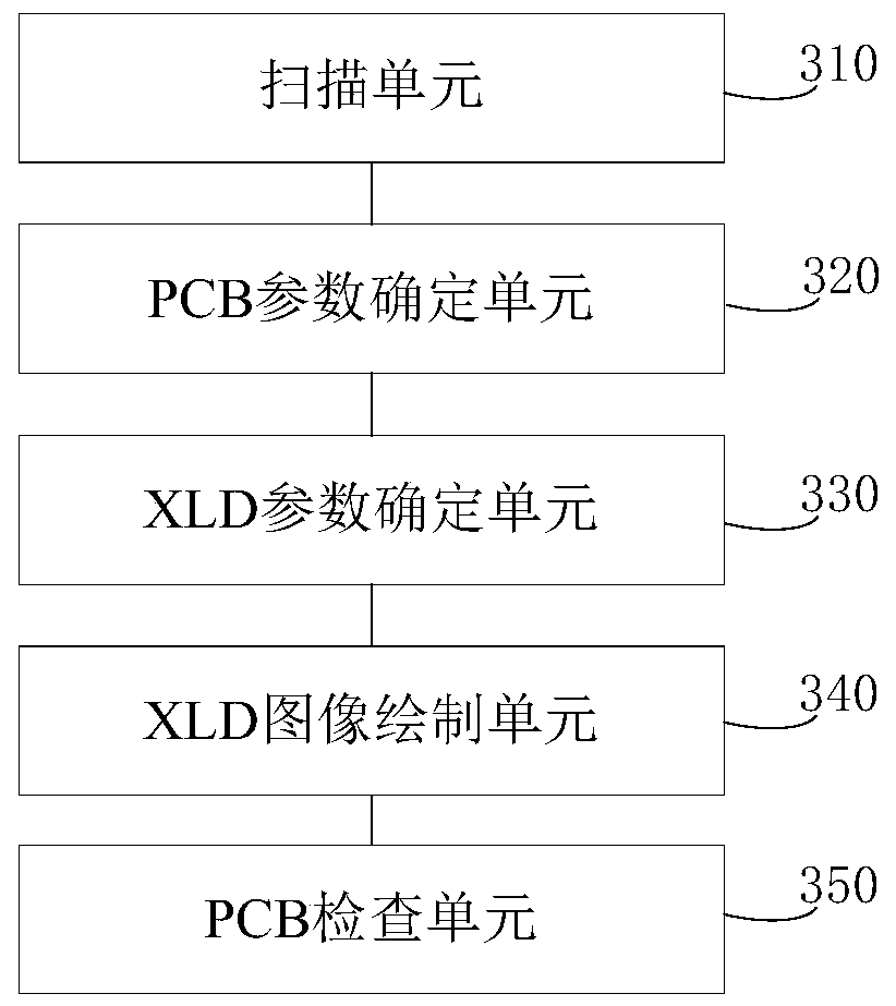
[0037] In order to solve the above problems, the present invention provides a method for improving PCB inspection accuracy, specifically, it relates to a method for converting Gerber files in RS-274X format into XLD files, and its purpose is to convert Gerber files into XLD files that are also vector graphics Format. Therefore, the error caused by the pixel size can be eliminated in the process...


PUM


Abstract

The invention discloses a method and system for improving PCB inspection precision, and the method comprises the steps: reading a Gerber file, and checking whether the Gerber file is in an RS-274X format or not; searching various Gerber file codes according to a Gerber file grammar rule to obtain parameter information of a Gerber file image; according to the parameter information of the Gerber file image, calculating parameters required for drawing the XLD image by adopting an interpolation point algorithm; and drawing an XLD image by using Halcon software according to the calculated parameters. Meanwhile, the invention further discloses a system for converting the Gerber file in the RS-274X format into the XLD file. When the technical scheme is applied to the AOI, precision errors causedby the sizes of the bit pixels are avoided, the method and system have the advantages of being high in precision, simple and efficient, and the PCB inspection precision is improved.

Description

technical field [0001] The invention relates to the field of optical detection, and more specifically, to a method and system for improving PCB inspection accuracy. Background technique [0002] The full name of AOI (Automated Optical Inspection) is automatic optical inspection, which is based on optical principles to detect common defects encountered in welding production. AOI is a new type of testing technology emerging, but it is developing rapidly, and many manufacturers have launched AOI testing equipment. When automatic detection, the machine automatically scans the printed circuit board (PCB) through the camera, collects the image, and obtains the corresponding Gerber format file, compares the tested solder joints with the qualified parameters in the database, and performs image processing , Check out the defects on the PCB, and display / mark the defects through the display or automatic signs for repairing by maintenance personnel. [0003] When obtaining the actual ...

Claims


Application Information

Patent Timeline
Patent Type & Authority Applications(China)
IPC IPC(8): G06T7/00G06T7/60G06T9/00G06T9/20G06F30/398
CPCG06T7/0006G06T7/60G06T9/008G06T9/20G06T2207/30141Y02P90/30
Inventor 夏珉夏楠卿胡海杨克成
Owner HUAZHONG UNIV OF SCI & TECH
Why Eureka
Try Eureka