

Photoetching process method
A lithography process and photoresist technology, applied in the field of lithography process, can solve the problems affecting the line width uniformity of wafer graphics, etc., and achieve the effect of eliminating the line width difference of exposed graphics and improving the line width uniformity
- Summary
- Abstract
- Description
- Claims
- Application Information
AI Technical Summary
Problems solved by technology
Method used
Image

Examples
Embodiment Construction
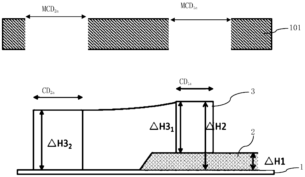
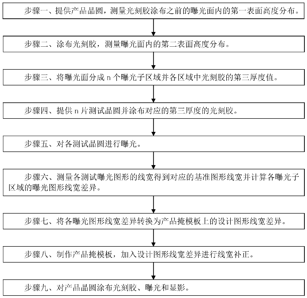
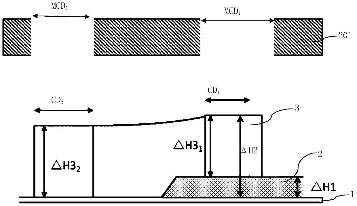
[0043] Such as figure 2 Shown is the flowchart of the photolithography process method of the embodiment of the present invention; as image 3 Shown is a schematic diagram of the exposure pattern formed on the uneven wafer surface by the photolithography process method of the embodiment of the present invention; as Figure 4 As shown, it is a schematic diagram of partitioning the exposure surface 4 by the lithography process method of the embodiment of the present invention; the lithography process method of the embodiment of the present invention includes steps:
[0044] Step 1, providing a product wafer 1 with a first substrate structure 3 formed on its surface, measuring the first surface height distribution in the exposure surface 4 of the product wafer 1 before photoresist coating, the first surface The height distribution is composed of the first surface height values of each position in the exposure surface 4, image 3 The value of the first surface height in is rep...
PUM
 Abstract
Description
Claims
Application Information