Non-contact measuring method for upper and lower layer copper thickness applied to pcb multilayer board

A non-contact, multi-layer board technology, applied in the field of measurement, can solve the problems of inability to measure the structure of multi-layer films, damage to the film body, and non-transparency of metal films.

Active Publication Date: 2021-07-09
陈建璋
View PDF9 Cites 0 Cited by
  • Summary
  • Abstract
  • Description
  • Claims
  • Application Information

AI Technical Summary

Problems solved by technology

However, the metal film is not light-transmitting, and the thickness of the coating is mostly measured using a destructive, contact-type four-point probe measurement method, and the contact measurement method will cause damage to the film body due to contact with the metal film , leading to the traditional measurement technology usually captures a part of the sample first, and measures it in a static manner. In addition, the accuracy of traditional measurement equipment can only measure the film thickness of a single metal layer, but cannot be used for multi-layer films. structure for measurement

Method used


Image

  • Non-contact measuring method for upper and lower layer copper thickness applied to pcb multilayer board
  • Non-contact measuring method for upper and lower layer copper thickness applied to pcb multilayer board
  • Non-contact measuring method for upper and lower layer copper thickness applied to pcb multilayer board

Examples


Embodiment Construction

[0025] The features and technical contents of the relevant patent applications of the present invention will be clearly presented in the following detailed description of preferred embodiments with reference to the drawings.

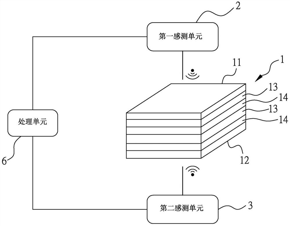
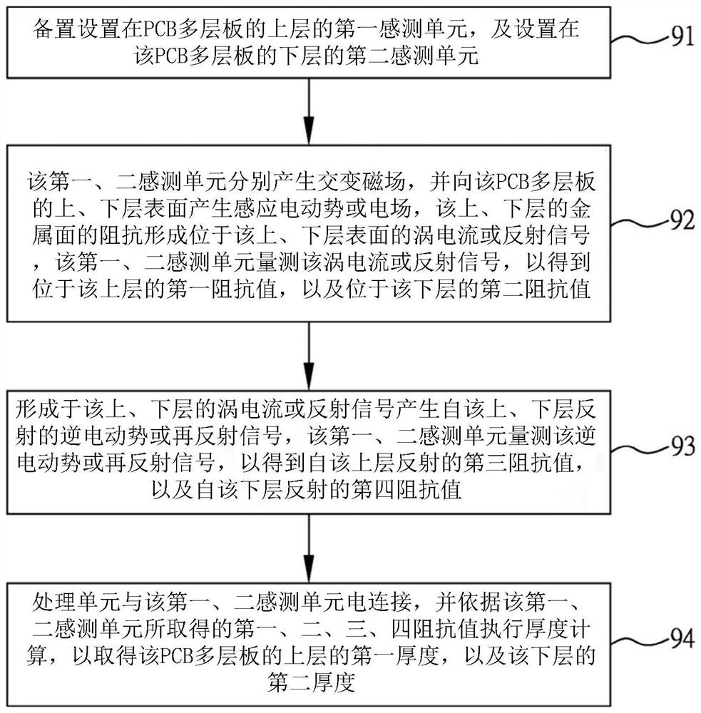
[0026] refer to figure 1 , 2 , which is a preferred embodiment of the non-contact method for measuring the copper thickness of the upper and lower layers of the PCB (Printed Circuit Board) multilayer board of the present invention, which includes the following steps.

[0027] First, proceed to step 91 , prepare the first sensing unit 2 disposed on the upper layer 11 of the PCB multilayer board 1 , and the second sensing unit 3 disposed on the lower layer 12 of the PCB multilayer board 1 . The measurement object of the measurement method of the present invention may be a PCB multilayer board 1 structure in which various surface coating materials are metal.

[0028] Here, the number of layers of the PCB multilayer board 1 is between 2 and 16 layers, and ...


PUM

PropertyMeasurementUnit
frequencyaaaaaaaaaa
frequencyaaaaaaaaaa

Abstract

A method for measuring the copper thickness of the non-contact upper and lower layers applied to a PCB multilayer board, comprising the following steps: firstly, a first sensing unit arranged on the upper layer of the PCB multilayer board, and a first sensing unit arranged on the lower layer are provided. Two sensing units, then the first and second sensing units generate induced electromotive force or electric field to the upper and lower surfaces, and the impedance of the upper and lower metal surfaces forms eddy currents or reflected signals, and the first and second sensing units The eddy current or reflected signal is measured to obtain the first impedance value and the second impedance value, and then the eddy current or reflected signal of the upper and lower layers generates a reflected back electromotive force or a re-reflected signal, and the first and second sensing units measure Measure the counter electromotive force or re-reflection signal to obtain the third impedance value and the fourth impedance value, and finally the processing unit performs thickness calculation according to the first, second, third, and fourth impedance values ​​to obtain the first thickness of the upper layer and the thickness of the lower layer second thickness.

Description

technical field [0001] The invention relates to a measurement method, in particular to a non-contact method for measuring the copper thickness of the upper and lower layers of a PCB multilayer board. Background technique [0002] With the continuous evolution of semiconductor process technology, metal coating process combined with etching or grinding process is widely used in the connection and conduction of integrated circuits, which has become an important key technology of advanced process. [0003] The traditional thin film measurement equipment mostly uses contact measurement technology to measure the thickness of metal thin films. However, the metal film is not light-transmitting, and the thickness of the coating is mostly measured using a destructive, contact-type four-point probe measurement method, and the contact measurement method will cause damage to the film body due to contact with the metal film , leading to the traditional measurement technology usually capt...

Claims


Application Information

Patent Timeline
Patent Type & Authority Patents(China)
IPC IPC(8): G01B7/06
CPCG01B7/06
Inventor 陈建璋
Owner 陈建璋
Why Eureka
Try Eureka