Three-dimensional heterogeneous integrated chip and preparation method thereof

An integrated chip and chip technology, applied in the direction of electrical components, electric solid devices, circuits, etc., can solve the problems of new memory application difficulties, computing system speed and safety limitations, etc., and achieve fast data exchange speed, increased difficulty, wire parasitic The effect of low capacitance

Pending Publication Date: 2020-02-28
SHANGHAI INST OF MICROSYSTEM & INFORMATION TECH CHINESE ACAD OF SCI
View PDF3 Cites 3 Cited by
  • Summary
  • Abstract
  • Description
  • Claims
  • Application Information

AI Technical Summary

Problems solved by technology

[0005] This application is to solve the technical problems that the speed and security of the computing system in the prior art are limited, and the application of new memory is difficult

Method used


Image

  • Three-dimensional heterogeneous integrated chip and preparation method thereof
  • Three-dimensional heterogeneous integrated chip and preparation method thereof
  • Three-dimensional heterogeneous integrated chip and preparation method thereof

Examples


Embodiment Construction

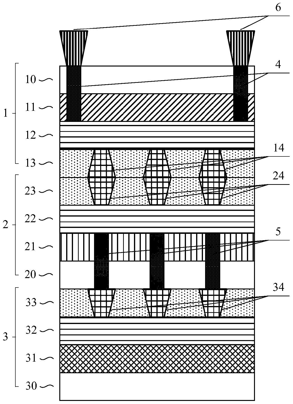
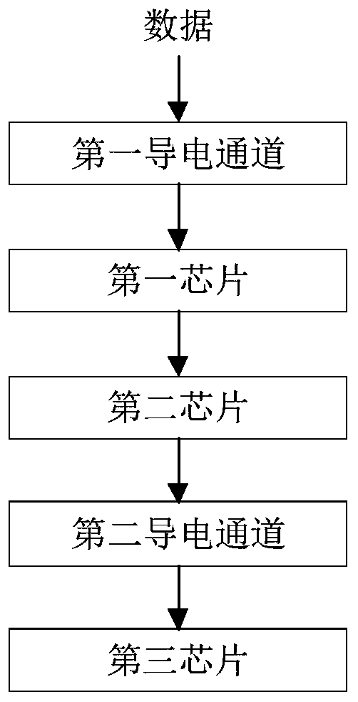
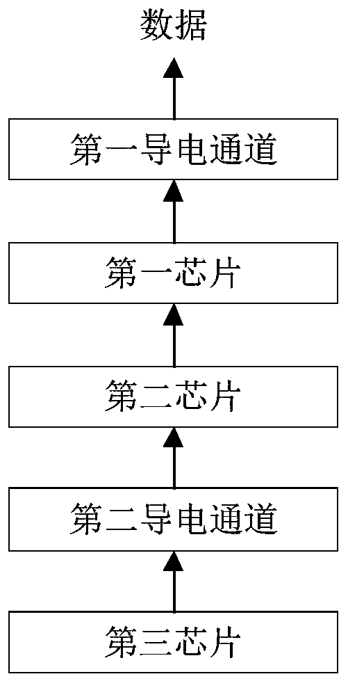
[0052] The technical solutions in the embodiments of the present application will be clearly and completely described below in conjunction with the drawings in the embodiments of the present application. Apparently, the described embodiments are only some of the embodiments of this application, not all of them. Based on the embodiments in this application, all other embodiments obtained by persons of ordinary skill in the art without creative efforts fall within the protection scope of this application.

[0053] Reference herein to "one embodiment" or "an embodiment" refers to a specific feature, structure or characteristic that may be included in at least one implementation of the present application. In the description of the embodiments of the present application, it should be understood that the orientations or positional relationships indicated by the terms "upper", "lower", "top", and "bottom" are based on the orientations or positional relationships shown in the drawing...


PUM


Abstract

The application provides a three-dimensional heterogeneous integrated chip and a preparation method thereof. The three-dimensional heterogeneous integrated chip includes a first chip and a second chip. The first chip includes a first substrate, a first active region layer, a first metal layer, a first dielectric layer and a first through hole. The first substrate, the first active area layer, thefirst metal layer, and the first dielectric layer are successively stacked and connected. The first through hole is disposed inside the first dielectric layer. The first through hole is connected to the outside of the first metal layer and the outside of the first dielectric layer. The second chip includes a second substrate, a first storage layer, a second dielectric layer, and a second through hole. The first storage layer is connected to the second substrate. The second dielectric layer is connected to the first storage layer. The second through hole is disposed inside the second dielectriclayer. The second through hole is connected to the outside of the second storage layer and the outside of the second dielectric layer. A first conductive channel is disposed inside the first chip. One end of the first conductive channel is connected to the first metal layer, the other end of the first conductive channel is connected to the outside of the first substrate. The first conductive channel is used as an input terminal or an output terminal of the second chip.

Description

technical field [0001] The invention relates to the technical field of integrated circuits, in particular to a three-dimensional heterogeneous integrated chip and a preparation method thereof. Background technique [0002] Under the classic computer architecture, storage and computing are separated, which is reflected at the board level. Storage chips and computing chips are independently packaged on circuit boards, and data is exchanged through board-level wires. However, the board-level wires have large diameters and large parasitic capacitances, which limit the speed of data transmission; exposed wires allow attackers to eavesdrop on wire signals and obtain keys, which poses a great security risk. Three-dimensional integrated circuits (3D-ICs) using wafer-wafer stacking are expected to solve this problem. [0003] According to the speed, the storage architecture is static random access memory (Static Random-Access Memory, SRAM), dynamic random access memory (Dynamic Rand...

Claims


Application Information

Patent Timeline
Patent Type & Authority Applications(China)
IPC IPC(8): H01L27/105H01L27/22H01L27/24
CPCH01L27/105H10B61/00H10B63/00H10B99/00
Inventor 宋志棠雷宇陈邦明
Owner SHANGHAI INST OF MICROSYSTEM & INFORMATION TECH CHINESE ACAD OF SCI
Why Eureka
Try Eureka