Radiation hardening silicon-based bipolar transistor structure based on self-built electric field and preparation method

A bipolar transistor and radiation hardening technology, which is applied in transistors, semiconductor/solid-state device manufacturing, circuits, etc., can solve the problems of gain reduction, increase of transistor recombination current, increase of recombination center on the surface of transistor base area, etc., to ensure device performance and reliability, mature and controllable process, low cost and process difficulty

Active Publication Date: 2020-02-28
XIAN MICROELECTRONICS TECH INST
View PDF6 Cites 0 Cited by
  • Summary
  • Abstract
  • Description
  • Claims
  • Application Information

AI Technical Summary

Problems solved by technology

[0003] When the silicon-based bipolar transistor is irradiated with the total dose, the radiation ionization effect will cause a large amount of radiation-induced positive charges to be generated in the silicon dioxide insulating layer on the surface of the transistor. When these positive charges move to the silicon-silicon dioxide interface, It will react with the dangling bonds at the interface to generate new interface states, increase the recombination center on the surface of the transistor base, increase the recombination current of the transistor, and decrease the gain, which will cause the transistor to fail under the action of total dose radiation

Method used


Image

  • Radiation hardening silicon-based bipolar transistor structure based on self-built electric field and preparation method
  • Radiation hardening silicon-based bipolar transistor structure based on self-built electric field and preparation method
  • Radiation hardening silicon-based bipolar transistor structure based on self-built electric field and preparation method

Examples


Embodiment 1

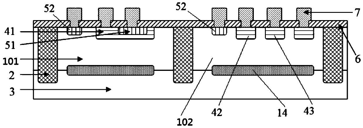
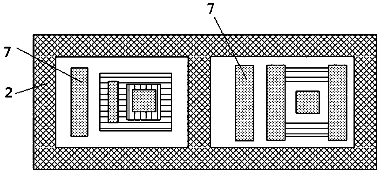
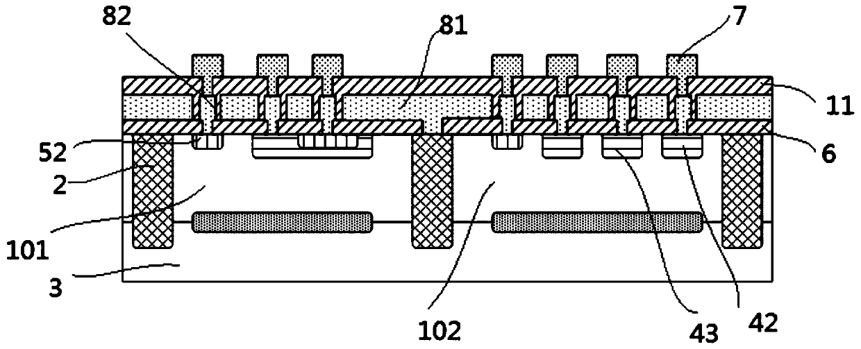
[0045] A radiation-hardened silicon-based bipolar transistor structure based on a self-built electric field, including a bipolar transistor body 100, a silicon dioxide insulating layer 6, a ground potential layer 8, an insulating dielectric layer 11, and circuit wiring interconnections arranged in sequence from bottom to top Layer 7. Wherein, the body of the bipolar transistor is a doped silicon wafer. The insulating layer 6 covers the upper surface of the bipolar transistor main body 100, and the silicon dioxide insulating layer 6 is provided with a ground potential electrode contact window and a bipolar transistor electrode lead-out contact window, and the upper surface of the silicon dioxide insulating layer 6 is covered with a ground potential layer 8 , the ground potential layer 8 includes a ground potential electrode 81 and a plurality of bipolar transistor lead-out electrodes 82; the ground potential layer 8 is provided with a groove for accommodating the terminal, and ...

Embodiment 2

[0059] A radiation-hardened silicon-based bipolar transistor structure based on a self-built electric field, including a bipolar transistor body 100, a silicon dioxide insulating layer 6, a ground potential layer 8, an insulating dielectric layer 11, and circuit wiring interconnections arranged in sequence from bottom to top Layer 7. Wherein, the body of the bipolar transistor is a doped silicon wafer. The insulating layer 6 covers the upper surface of the bipolar transistor main body 100, and the silicon dioxide insulating layer 6 is provided with a ground potential electrode contact window and a bipolar transistor electrode lead-out contact window, and the upper surface of the silicon dioxide insulating layer 6 is covered with a ground potential layer 8 , the ground potential layer 8 includes a ground potential electrode 81 and a plurality of bipolar transistor lead-out electrodes 82; the ground potential layer 8 is provided with a groove for accommodating the terminal, and ...


PUM

PropertyMeasurementUnit
Thicknessaaaaaaaaaa
Thicknessaaaaaaaaaa
Thicknessaaaaaaaaaa

Abstract

The invention discloses a radiation hardening silicon-based bipolar transistor structure based on a self-built electric field and a preparation method. The bipolar transistor structure is formed through multilayer wiring: through the multilayer wiring, a ground potential layer communicated with the lowest potential is formed on the surface of a transistor so as to form the self-built electric field pointing to the ground potential layer in a silicon dioxide insulating layer between each doped region of the transistor and the ground potential layer. The self-built electric field inhibits positive charges generated by total dose radiation in the silicon dioxide insulating layer from moving to a silicon-silicon dioxide interface, so that the number of the positive charges induced by radiationin reaching the silicon-silicon dioxide interface and forming a new interface state is reduced, and the total dose radiation resistance of the bipolar transistor is improved.

Description

technical field [0001] The invention belongs to the technical field of silicon-based transistors, and in particular relates to a radiation-hardened silicon-based bipolar transistor structure and a preparation method based on a self-built electric field. Background technique [0002] Conventional silicon-based bipolar transistors include NPN transistors and PNP transistors. Their structures are selectively doped with P-type or N-type impurities in different regions of the silicon substrate or epitaxial layer to form NPN or PNP structures, and are realized by wires. The final transistor structure also needs to cover a layer of silicon dioxide on the surface of the transistor as an insulating layer between the metal lead and the doped region of the transistor to avoid short circuits between different doped regions of the transistor through metal connections. [0003] When the silicon-based bipolar transistor is irradiated with the total dose, the radiation ionization effect wil...

Claims


Application Information

Patent Timeline
IPC IPC(8): H01L29/06H01L21/331H01L29/73
CPCH01L29/66234H01L29/73H01L29/0603Y02P70/50
Inventor 王清波薛东风赵杰薛智民孙有民杜欣荣卓青青
Owner XIAN MICROELECTRONICS TECH INST
Why Eureka
Try Eureka