GaAs-based high-power laser preparation method

A technology of high-power lasers and equipment, applied in the direction of lasers, laser components, semiconductor lasers, etc., can solve problems that affect the reliability and life of semiconductor lasers, chip thermal damage, etc., to ensure current expansion and optical characteristics, improve reliability Effect

Active Publication Date: 2020-02-28
Shandong Huaguang Optoelectronics Co. Ltd.
View PDF9 Cites 2 Cited by
  • Summary
  • Abstract
  • Description
  • Claims
  • Application Information

AI Technical Summary

Problems solved by technology

The reflected laser may also directly irradiate the semiconductor laser chip, resulting in thermal damage to the chip. The above problems will seriously affect the reliability and life of the semiconductor laser, and put forward higher requirements for the heat dissipation capacity of the semiconductor laser chip

Method used


Image

  • GaAs-based high-power laser preparation method

Examples


preparation example Construction

[0034] A method for preparing a GaAs-based high-power laser, comprising the steps of:

[0035] a) The GaAs substrate is placed in the growth chamber of the MOCVD equipment, baked in an H2 gas environment, and AsH3 gas is fed after baking to remove water and oxygen on the surface of the substrate to complete the surface treatment;

[0036] b) Lower the temperature to 750±20°C, pass the AsH3 gas and then pass the TMAl gas with the defined composition, stop the TMAl gas and pass the TMGa gas with the defined composition after an interval of 1-5 seconds, with an interval of 1-10 seconds Seconds later, stop feeding AsH3 gas and TMGa gas to stop growth for 1-50s;

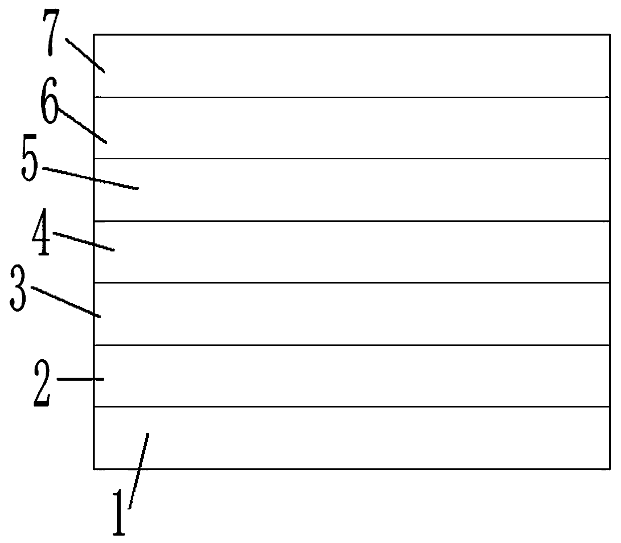
[0037] c) Repeat step b) until a GaAs low-temperature buffer layer 1 with a specified thickness is grown on the substrate;

[0038] d) Keep the temperature at 750±20°C, pass the AsH3 gas and then pass the TMAl gas with the defined composition, stop the TMAl gas after an interval of 1-5 seconds and pass the TMGa gas with ...

Embodiment 1

[0052] The temperature during baking in step a) is 800±20° C., and the baking time is 30 minutes.

Embodiment 2

[0054] The thickness of the GaAs low-temperature buffer layer 1 in step c) is 50-500 nm. The doping concentration is 1E17-5E18 atoms / . Preferably, the GaAs low-temperature buffer layer 1 has a thickness of 100 nm and a doping concentration of 1E18 atoms / .


PUM

PropertyMeasurementUnit
thicknessaaaaaaaaaa

Abstract

The invention provides a GaAs-based high-power laser preparation method. When a GaAs low temperature buffer layer, a AlxGayAs lower confinement layer, a AlGaAs lower waveguide layer, a quantum well luminous region, a AlGaAs upper waveguide layer, a AlxGayAs upper confinement layer and a GaAs cap layer are grown, AsH3 gas is first introduced and then TMAL gas defined by component is introduced, then the introduction of TMAL gas is stopped and the TMGa gas defined by the component is introduced with intervals of 1-5s, and the introduction of the AsH3 gas is stopped and growth of TMGa gas is stopped by 1-50s after the interval of 1-10s, and the thickness requirement of each layer growth is reached through periodic circulation. The structure can accurately control the epitaxial growth with onemonoatomic layer per cycle, the epitaxial surface is more atomic and flat and the thickness of the epitaxial layer is only determined by the number of epitaxial periods so as to solve the problems ofchemical weather growth sensitive to temperature, beam current size and the like, grow high-quality thin film materials at lower temperature, ensure current expansion and optical characteristics andimprove reliability and stability of the device.

Description

technical field [0001] The invention relates to the technical field of laser manufacturing, in particular to a method for preparing a GaAs-based high-power laser. Background technique [0002] High-power semiconductor lasers have the advantages of small size, light weight, high reliability, long life, and low cost. The core device with many achievements, wide penetration of disciplines, and wide application range has been widely used in various fields of the national economy such as laser processing, Laser medical treatment, laser display and scientific research fields. [0003] GaAs-based high-power lasers are one of the packaging structures of semiconductor lasers. The specific structure is to arrange single-Bar semiconductor lasers evenly along the direction of the slow axis. This horizontal array packaging structure is often used as a pump source for solid-state lasers. Multiple semiconductor lasers with a horizontal array structure are evenly arranged around the crysta...

Claims


Application Information

Patent Timeline
Patent Type & Authority Applications(China)
IPC IPC(8): H01S5/34H01S5/343C23C16/30C23C16/455
CPCC23C16/301C23C16/45527H01S5/34H01S5/34353
Inventor 张新李志虎朱振徐现刚
Owner Shandong Huaguang Optoelectronics Co. Ltd.
Why Eureka
Try Eureka