Method for planarizing virtual gate

A planarization method and technology of dummy gates, which are applied in the fields of electrical components, semiconductor/solid-state device manufacturing, circuits, etc., can solve problems such as affecting device performance and different heights of polysilicon dummy gates 104, so as to improve device performance and improve height consistency. , The effect of improving product yield

Active Publication Date: 2020-03-06
SHANGHAI HUALI INTEGRATED CIRCUTE MFG CO LTD
View PDF6 Cites 1 Cited by
  • Summary
  • Abstract
  • Description
  • Claims
  • Application Information

AI Technical Summary

Problems solved by technology

In the end, the height of the polysilicon dummy gate 104 will be different in each region, which will affect the performance of the device in the end.

Method used


Image

  • Method for planarizing virtual gate
  • Method for planarizing virtual gate
  • Method for planarizing virtual gate

Examples


Embodiment Construction

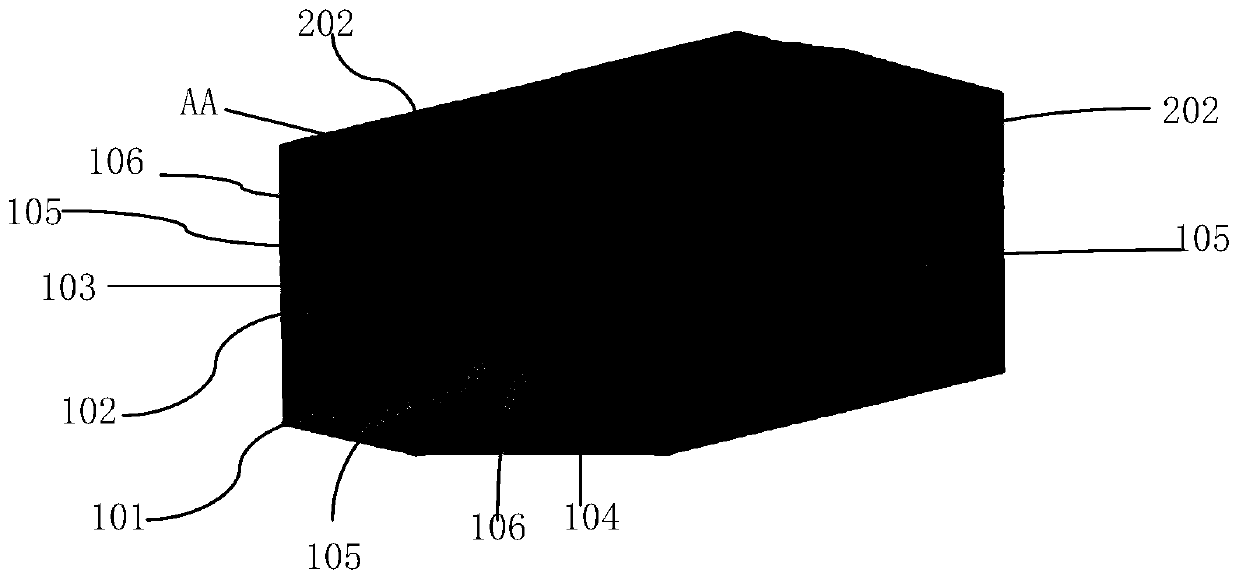
[0066] Such as image 3 As shown, it is a flow chart of the planarization method of the virtual gate in the embodiment of the present invention; as Figure 4A to Figure 4D As shown, it is a schematic diagram of the cross-sectional structure of the device in each step of the planarization method of the virtual gate in the embodiment of the present invention. For the position of the cross-section, please refer to Figure 1C AA line in the embodiment of the present invention, the planarization method of the virtual gate includes the following steps:

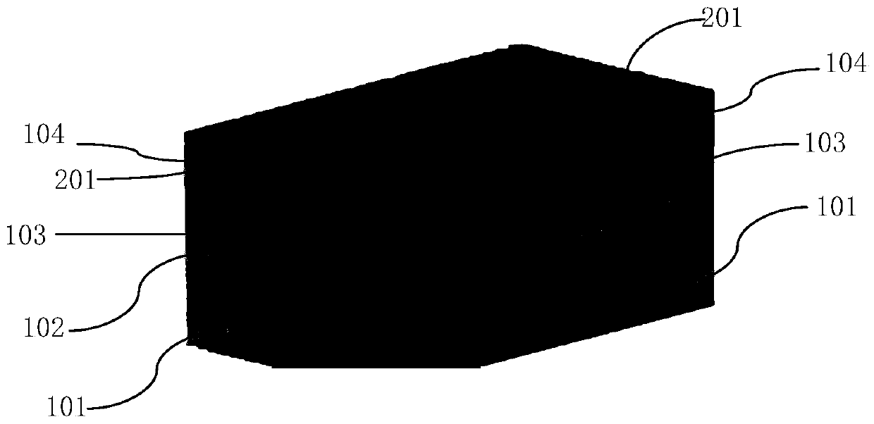
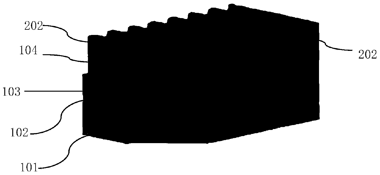
[0067] Step 1, such as Figure 4A As shown, a dummy gate formed by overlapping the first gate dielectric layer 301 and the polysilicon dummy gate 104 is formed on the semiconductor substrate 101; the semiconductor substrate 101 has an uneven area, and the surface of the polysilicon dummy gate 104 is also Uneven, for example, there is a recessed region 201 on the surface of the polysilicon dummy gate 104 .

[0068] In the embodime...


PUM


Abstract

The invention discloses a method for planarizing a virtual gate, comprising the steps of: forming a virtual gate formed by superposing a first gate dielectric layer and a polycrystalline silicon dummygate; forming a zeroth interlayer film; performing a first chemical mechanical polishing process in such a way that a polishing rate of the zeroth interlayer film is greater than a polishing rate ofthe polycrystalline silicon dummy gate; performing a second planarization process in such a way that a removal rate of the zeroth interlayer film is less than a removal rate of the polycrystalline silicon dummy gate, wherein a surface of the zeroth interlayer film in a surface recessed area of the polycrystalline silicon dummy gate is flush with a surface of the zeroth interlayer film outside thesurface recessed area after the planarization; and performing a non-selective polycrystalline silicon thinning process. The method can completely open the uneven top surface of the virtual gate so asto completely remove the virtual gate and improve the product yield, and can improve the height consistency of the virtual gate, and the device performance.

Description

technical field [0001] The invention relates to a method for manufacturing a semiconductor integrated circuit, in particular to a method for planarizing a dummy gate. Background technique [0002] As the geometry of large-scale integrated circuits continues to shrink, especially after entering the fin transistor (FINFET) process, the local non-uniformity of chemical mechanical polishing (CMP) has become an increasingly serious problem that needs to be solved urgently. In the FINFET process, if the local planarization of the dummy gate poly of the dummy gate cannot meet the requirements, in the poly open polishing (POP) process, the polysilicon line of some dummy gates (dummy polyline) The silicon nitride (SiN) on it cannot be completely cleaned, and various work function metals cannot be filled in the subsequent process, resulting in yield loss. [0003] The local height planarization of the virtual gate is not good, and the heights of devices at different positions will al...

Claims


Application Information

Patent Timeline
Patent Type & Authority Applications(China)
IPC IPC(8): H01L21/336H01L21/28
CPCH01L29/66545H01L29/66795H01L21/28008
Inventor 胡宗福龚昌鸿陈建勋
Owner SHANGHAI HUALI INTEGRATED CIRCUTE MFG CO LTD
Why Eureka
Try Eureka