Power supply module packaging structure and power supply module packaging method
A power module and packaging structure technology, which is applied in the direction of circuits, electrical components, and electric solid devices, can solve the problems of poor heat dissipation performance and large packaging structure size, and achieve the effect of improving heat dissipation performance and reducing size
- Summary
- Abstract
- Description
- Claims
- Application Information
AI Technical Summary
Problems solved by technology
Method used
Image


Examples
Embodiment 1
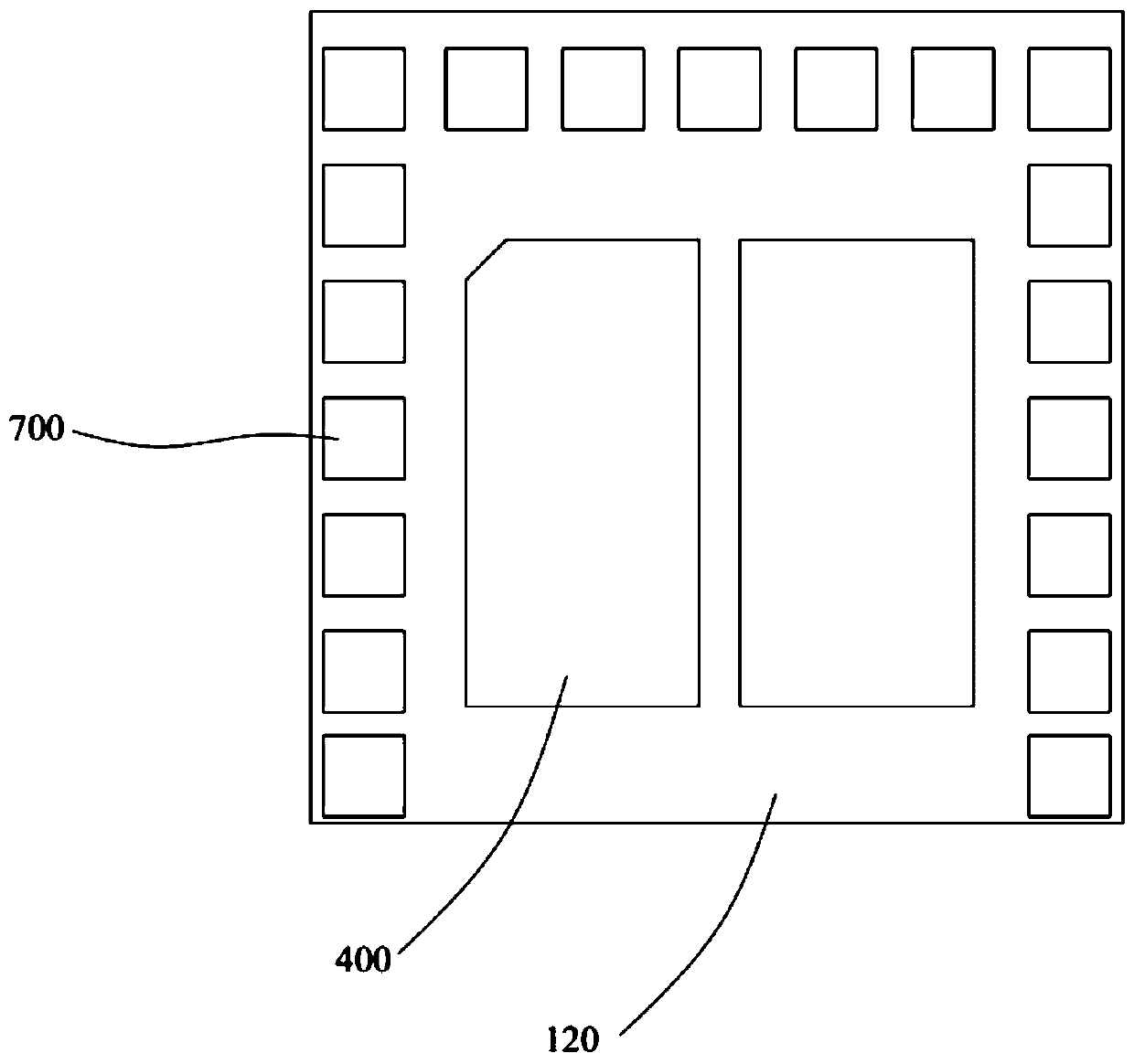
[0062] The package structure of the power module in this embodiment includes a substrate 100, a DC-DC chip 200, a capacitor, a MOS tube 320, a PIN pin 600, an inductor 400, and a plastic sealing part 500. The DC chip 200, the capacitor and the MOS tube 320 are installed on the top surface 110 of the substrate 100, the PIN needle 600 and the inductor 400 are installed on the bottom surface 120 of the substrate 100, and the plastic sealing part 500 includes the first plastic sealing layer 510 and the filling The second plastic packaging layer 520 is sealed on the bottom surface 120 , the DC-DC chip 200 , the capacitor, and the MOS tube 320 are packaged in the first plastic packaging layer 510 , and the PIN needle 600 and the inductor 400 are packaged in the second plastic packaging layer 520 . The second plastic sealing layer 520 is a compression molding layer, the thickness of the inductor 400 is equal to the thickness of the second plastic sealing layer 520, one end of the PIN ...
Embodiment 2
[0071] The package structure of the power module in this embodiment includes a substrate 100, an AC-DC chip 200, a capacitor, a PIN pin 600, an inductor 400, and a plastic sealing part 500. The capacitor is installed on the top surface 110 of the substrate 100, the PIN pin 600 and the inductor 400 are installed on the bottom surface 120 of the substrate 100, and the plastic sealing part 500 includes a first plastic sealing layer 510 potted on the top surface 110 and a second plastic sealing layer potted on the bottom surface 120. The layer 520 , the AC-DC chip 200 and the capacitor are packaged in the first plastic packaging layer 510 , and the PIN pin 600 and the inductor 400 are packaged in the second plastic packaging layer 520 . The second plastic sealing layer 520 is a compression molding layer, the thickness of the inductor 400 is equal to the thickness of the second plastic sealing layer 520, one end of the PIN pin 600 is connected to the substrate 100, and the other end...
PUM
 Abstract
Description
Claims
Application Information
PatSnap Eureka turns technology decisions into work you can execute. Powered by our Innovation Knowledge Graph, it runs expert workflows across engineering, life sciences, materials and intellectual property. Get your review-ready output in minutes.


