Laser and silicon optical chip integrated structure and preparation method thereof

A technology of silicon photonic chips and lasers, applied in light guides, optics, instruments, etc., can solve the problems of high alignment accuracy requirements and low coupling efficiency, and achieve the effects of low alignment accuracy, good heat dissipation performance, and high coupling efficiency

Active Publication Date: 2020-04-03
SHANGHAI IND U TECH RES INST
View PDF6 Cites 16 Cited by
  • Summary
  • Abstract
  • Description
  • Claims
  • Application Information

AI Technical Summary

Problems solved by technology

[0003] In view of the shortcomings of the prior art described above, the purpose of the present invention is to provide a laser and silicon photonic chip integration structure and its preparation method, which are used to solve the alignment accuracy existing in the laser and silicon photonic chip integration technology in the prior art High requirements and low coupling efficiency

Method used


Image

  • Laser and silicon optical chip integrated structure and preparation method thereof
  • Laser and silicon optical chip integrated structure and preparation method thereof
  • Laser and silicon optical chip integrated structure and preparation method thereof

Examples


Embodiment 1

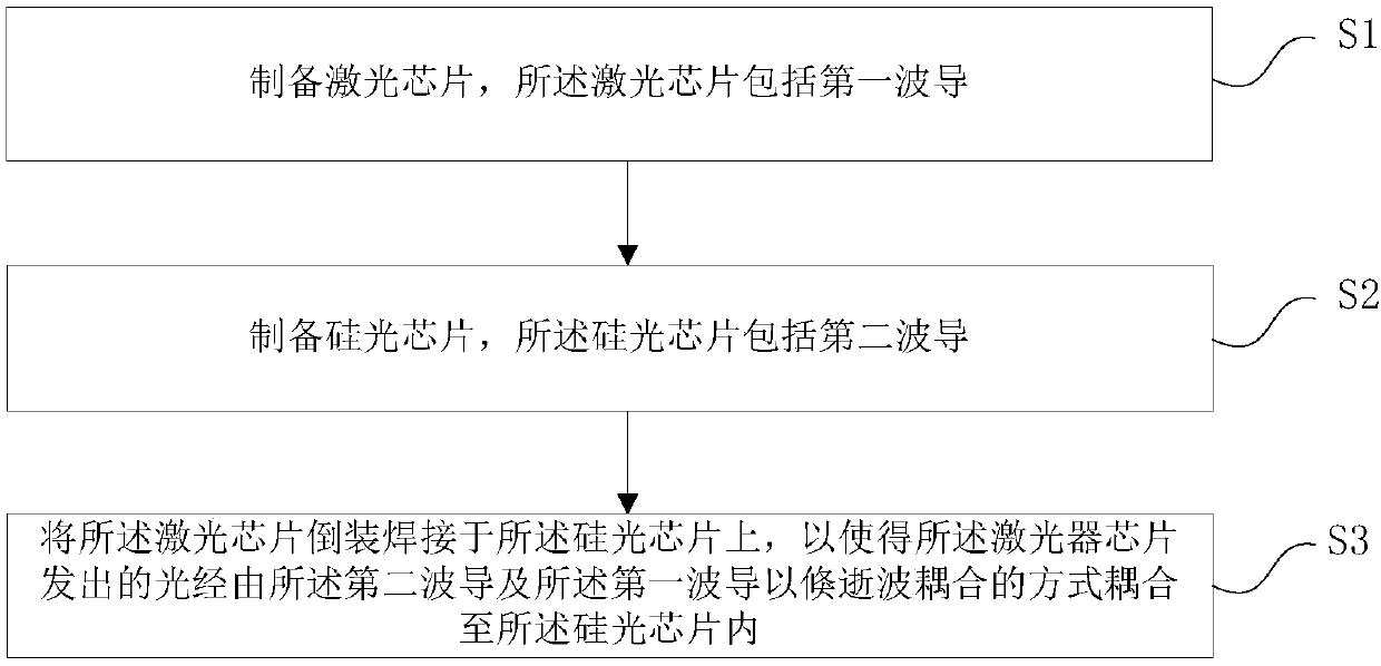
[0095] see figure 1 , the present invention provides a method for preparing an integrated structure of a laser and a silicon photonic chip, the method for preparing an integrated structure of a laser and a silicon photonic chip includes the following steps:

[0096] Prepare a laser chip 1, the laser chip 1 includes a first waveguide 13;

[0097] Prepare a silicon photonics chip 2, the silicon photonics chip 2 includes a second waveguide;

[0098] The laser chip 1 is flip-chip welded on the silicon photonics chip 2, so that the light emitted by the laser chip 1 is coupled to the Inside the silicon photonics chip 2 .

[0099] As an example, the laser chip 1 can be prepared first, and then the silicon photonic chip 2 can be prepared, or the silicon photonic chip 2 can be prepared first, and then the laser chip 1 can be prepared. That is, the order of preparing the laser chip 1 and the silicon photonics chip 2 can be interchanged.

[0100] As an example, see Figure 2 to Figu...

Embodiment 2

[0136] Please combine Figure 2 to Figure 18 read on Figure 19 to Figure 20 , the present invention also provides an integrated structure of a laser and a silicon photonic chip, wherein the integrated structure of a laser and a silicon photonic chip includes:

[0137] A laser chip 1, the laser chip 1 comprising a first waveguide 13;

[0138] A silicon photonics chip 2, the silicon photonics chip 2 includes a second waveguide, the second waveguide and the first waveguide 13 couple the light emitted by the laser chip 1 to the silicon photonics by evanescent wave coupling Chip 2 inside.

[0139]As an example, the first waveguide 13 includes a first inverted tapered waveguide portion 131, a rectangular waveguide portion 132, and a second inverted tapered waveguide portion 133 that are integrally connected in sequence; the second waveguide includes a first silicon nitride waveguide 25 , the second silicon nitride waveguide 23 and the silicon waveguide 21; wherein, the first sil...


PUM

PropertyMeasurementUnit
widthaaaaaaaaaa
lengthaaaaaaaaaa
thicknessaaaaaaaaaa

Abstract

The invention provides a laser and silicon optical chip integrated structure and a preparation method thereof. The laser and silicon optical chip integrated structure comprises a laser chip which comprises a first waveguide, and a silicon optical chip which comprises a second waveguide, wherein the second waveguide and the first waveguide couple the light emitted by the laser chip into the siliconoptical chip in an evanescent wave coupling manner. According to the laser and silicon optical chip integrated structure prepared by the invention, the first waveguide in the laser and the second waveguide in the silicon optical chip couple the light emitted by the laser into the silicon optical chip in the evanescent wave coupling manner, compared with the end face coupling in the prior art, thecoupling mode has lower requirement for alignment accuracy in the flip-chip bonding process, and still has higher coupling efficiency even under the actual process condition that alignment has errors.

Description

technical field [0001] The invention belongs to the technical field of hybrid integration, and in particular relates to an integrated structure of a laser and a silicon optical chip and a preparation method thereof. Background technique [0002] Lasers are the light source of silicon photonic chips. Since silicon materials cannot emit light by themselves, how to integrate lasers (for example, III-V lasers) with silicon photonic chips is the key to the development of optical transceiver modules. The current integration technology of lasers and silicon photonic chips mainly consists of three types: one is monolithic integration, that is, the laser is directly grown on the silicon substrate through epitaxy; the other is heterogeneous integration, that is, the laser chip is bonded to the silicon photonic chip Heterogeneous integration of Group III and V materials with silicon photonic chips by way of combination, and then preparation of lasers; third is hybrid integration, that ...

Claims


Application Information

Patent Timeline
Patent Type & Authority Applications(China)
IPC IPC(8): G02B6/42
CPCG02B6/4291
Inventor 蔡艳余明斌
Owner SHANGHAI IND U TECH RES INST
Why Eureka
Try Eureka