Display substrate, manufacturing method thereof and spliced display device

A technology for display substrates and base substrates, which is applied in the direction of identification devices, instruments, semiconductor devices, etc., can solve the problems of non-uniform light patterns of light-emitting chips, inability of viewers to see the picture clearly, color differences, etc., to achieve good display effect, Good display effect, high brightness contrast effect

Active Publication Date: 2020-04-07
BOE TECH GRP CO LTD +1
View PDF11 Cites 14 Cited by
  • Summary
  • Abstract
  • Description
  • Claims
  • Application Information

AI Technical Summary

Problems solved by technology

[0003] However, in the design of the small-pitch light diode (Mini LED) display on the glass substrate, the following pain points need to be considered: first, the reflection of ambient light, the reflectivity of the glass itself is high, when the ambient light hits the glass Reflection will occur on the surface of the glass, which may cause the viewer to not see the picture clearly. In addition, the reflectivity of various places on the glass (such as pixel positions, between pixels, and glass splicing) is different, which may easily lead to different degrees of blurring in the picture. Distortion; second, the light efficiency needs to be improved, and the light output efficiency of the LED needs to be increased to reduce power consumption; third, the color shift problem of large viewing angles, refer to figure 1 , the red, green and blue (RGB) light-emitting chip in a small package does not emit uniform light patterns, and color differences are prone to appear when viewed from different angles

Method used


Image

  • Display substrate, manufacturing method thereof and spliced display device
  • Display substrate, manufacturing method thereof and spliced display device
  • Display substrate, manufacturing method thereof and spliced display device

Examples


Embodiment Construction

[0052] The following describes the embodiments of the present invention in detail, and those skilled in the art will understand that the following embodiments are intended to explain the present invention, and should not be regarded as limiting the present invention. Unless otherwise specified, in the following examples that do not explicitly describe specific techniques or conditions, those skilled in the art can carry out according to commonly used techniques or conditions in this field or according to product instructions.

[0053] In one aspect of the invention, the invention provides a display substrate.

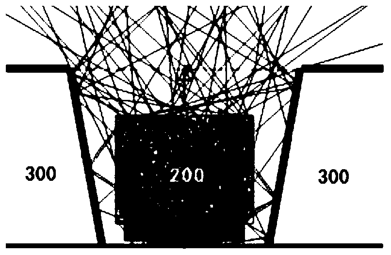
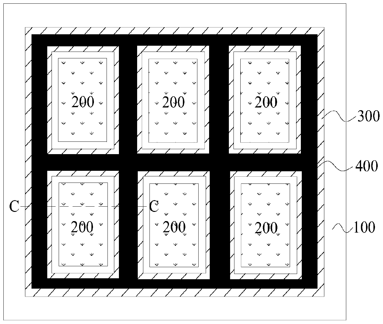
[0054] According to an embodiment of the present invention, refer to image 3 and Figure 4, the display substrate includes a plurality of base substrates 100, a plurality of light-emitting chips 200, a reflective wall 300 and a first black matrix layer 400; wherein, a plurality of base substrates 100 are spliced ​​to form a display substrate; a plurality of light-emit...


PUM

PropertyMeasurementUnit
particle diameteraaaaaaaaaa
thicknessaaaaaaaaaa

Abstract

The invention provides a display substrate, a manufacturing method thereof and a spliced display device. The display substrate comprises: a plurality of substrate base plates which are spliced to formthe display substrate; a plurality of light-emitting chips arranged on one side of the substrate base plate; a reflection retaining wall arranged between any two adjacent light-emitting chips; and afirst black matrix layer arranged on the surface, far away from the substrate, of the reflection retaining wall. According to the display substrate, the reflection retaining wall is arranged between any two adjacent light-emitting chips, so that the problem of large-view-angle color cast is solved, the light efficiency of the light-emitting chips is improved, the first black matrix layer is additionally arranged on the upper surface of the reflection retaining wall, reflection of the reflection retaining wall to ambient light is weakened, the brightness contrast ratio is improved, and the display effect is better.

Description

technical field [0001] The present invention relates to the field of display technology, in particular, the present invention relates to a display substrate, a manufacturing method thereof, and a spliced ​​display device. Background technique [0002] At this stage, the design of splicing display is becoming more and more popular, especially the large-size display products that are seamlessly spliced ​​after packaging small light-emitting chips (Mini or Micro). Because this technology is still in the stage of technology research and development, splicing Displayed processing optics also vary. [0003] However, in the design of the small-pitch light diode (Mini LED) display on the glass substrate, the following pain points need to be considered: first, the reflection of ambient light, the reflectivity of the glass itself is high, when the ambient light hits the glass Reflection will occur on the surface of the glass, which may cause the viewer to not see the picture clearly....

Claims


Application Information

Patent Timeline
Patent Type & Authority Applications(China)
IPC IPC(8): H01L33/60H01L33/48H01L33/58H01L25/075G09F9/302G09F9/33
CPCG09F9/3026G09F9/33H01L25/0753H01L33/48H01L33/58H01L33/60H01L2933/0033H01L2933/0058
Inventor 张功涛卢元达禹璐桑建
Owner BOE TECH GRP CO LTD
Why Eureka
Try Eureka