A thin film lithium niobate single polarization waveguide and its preparation method

A thin-film waveguide and lithium niobate technology, applied in the field of integrated photonics, can solve the problems of large-scale dense integration of lithium niobate single-polarization waveguides, complex process flow, etc., to improve mass production capacity, simplify process flow, and limit capacity strong effect

Active Publication Date: 2021-05-18
HUAZHONG UNIV OF SCI & TECH
View PDF6 Cites 0 Cited by
  • Summary
  • Abstract
  • Description
  • Claims
  • Application Information

AI Technical Summary

Problems solved by technology

[0004] In view of the defects of the prior art, the purpose of the present invention is to provide a thin-film lithium niobate single polarization waveguide and its preparation method, aiming to solve the problems that the existing lithium niobate single polarization waveguide is difficult to large-scale dense integration and the process flow is relatively complicated

Method used


Image

  • A thin film lithium niobate single polarization waveguide and its preparation method
  • A thin film lithium niobate single polarization waveguide and its preparation method
  • A thin film lithium niobate single polarization waveguide and its preparation method

Examples


Embodiment 1

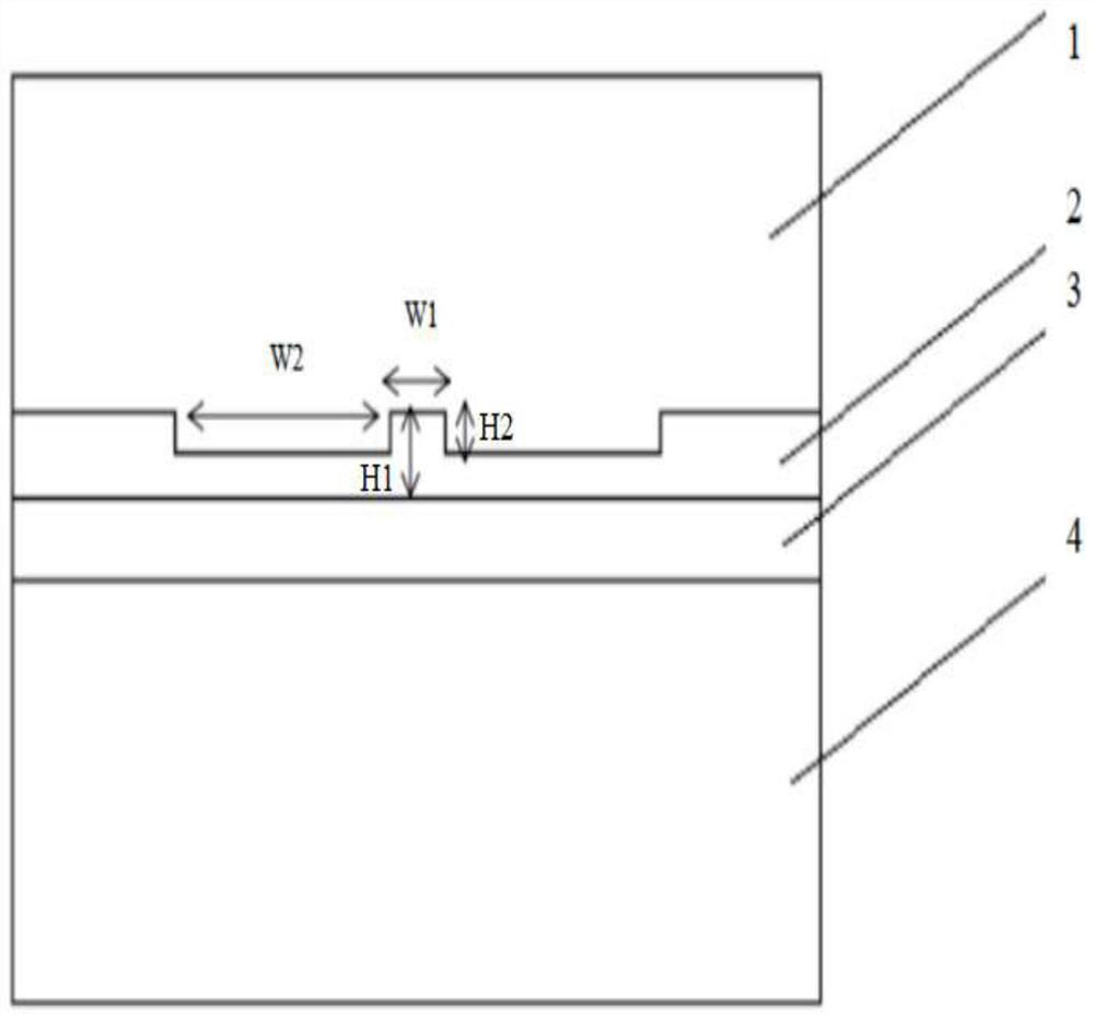
[0033] Figure 1-2 Shown is a schematic structural view of the thin-film lithium niobate single-polarization waveguide of this embodiment. The thin-film lithium niobate single-polarization waveguide of this embodiment comprises a silicon nitride upper cladding layer 1, a thin-film lithium niobate waveguide core layer 2, a silicon dioxide lower cladding layer 3 and Quartz substrate 4. The main structure of this embodiment is an X-cut Y-pass thin-film lithium niobate ridge waveguide. Preferably, the entire single-polarization optical circuit adopts the same single-polarization waveguide design.

[0034] The ridge width W1 and etching depth H2 of the thin-film lithium niobate waveguide core layer are determined by FDE simulation, and the widths of the grooves on both sides of the waveguide are determined by FDTD simulation. The total thickness H1 of the lithium niobate thin film is a fixed value. When the width W1 and the etching depth H2 are smaller than their theoretical ma...

Embodiment 2

[0044] The structural schematic diagram of the thin-film lithium niobate single-polarization waveguide of this embodiment can still refer to Figure 1-2 . The thin-film lithium niobate single-polarization waveguide of this embodiment includes a silicon dioxide upper cladding layer, a thin-film lithium niobate ridge waveguide core layer, a silicon dioxide lower cladding layer, and a silicon substrate. The main structure of this embodiment is an X-cut Y-pass thin-film lithium niobate ridge waveguide.

[0045] The preparation method of the thin-film lithium niobate single-polarization ridge waveguide of this embodiment comprises the following steps:

[0046] S1. Prepare thin film lithium niobate on insulator (Lithium niobate on insulator, LNOI)

[0047] S2: Cover a layer of metal material with conventional EBE (Electron Beam Evaporation, EBE) on the lithium niobate film, and expose the groove-shaped areas on both sides of the ridge-shaped waveguide protrusion structure on the ...


PUM

PropertyMeasurementUnit
widthaaaaaaaaaa
depthaaaaaaaaaa
widthaaaaaaaaaa

Abstract

The invention discloses a thin-film lithium niobate single-polarization waveguide and a preparation method thereof, belonging to the field of integrated photonics. The waveguide includes an upper cladding layer, a lithium niobate thin film waveguide core layer, a lower cladding layer and a substrate layer from top to bottom; the lithium niobate thin film waveguide core layer includes a ridge waveguide and grooves on both sides of the ridge waveguide shaped area; the width and etching depth of the ridge waveguide are less than the cut-off value of the TM0 mode, and the TM0 mode in the ridge waveguide cross-couples with the TE1 mode in the grooved area; the width of the grooved area is selected so that from The TMO mode in the ridge waveguide is coupled to the TE1 mode of the groove-shaped regions on both sides and the TMO mode leaked into the groove-shaped regions is coherent and constructive. By optimizing the geometric parameters of the micro-nano optical waveguide structure, a waveguide structure that only supports the stable transmission of TE0 mode is obtained. The thin-film lithium niobate single-polarization waveguide in the invention has a strong ability to limit the light field, improves the integration degree of the device, and simplifies the process flow.

Description

technical field [0001] The invention belongs to the field of integrated photonics, and more specifically relates to a thin-film lithium niobate single-polarization waveguide and a preparation method thereof. Background technique [0002] Microelectronics technology represented by VLSI has developed to a very high level. One of the directions to further improve the performance of integrated circuits is to introduce light with faster propagation speed and larger information capacity into integrated circuits to form optoelectronic integration. In the field of integrated photonics, the device used to process the polarization state is the key device that constitutes the polarization-dependent integrated optical circuit. The design of the single polarization waveguide is compatible with the design and process methods of other integrated photonics devices. When all the waveguides of the integrated optical circuit adopt the single polarization waveguide design, the signal light of t...

Claims


Application Information

Patent Timeline
Patent Type & Authority Patents(China)
IPC IPC(8): G02B6/10G02B6/126G02B6/136
CPCG02B6/10G02B6/126G02B6/136G02B2006/1204G02B2006/12097G02B2006/12176
Inventor 夏金松刘宇恒曾成
Owner HUAZHONG UNIV OF SCI & TECH
Why Eureka
Try Eureka