Thin-film lithium niobate single-polarization waveguide and preparation method thereof
A technology of thin-film waveguide and lithium niobate, which is applied in the field of integrated photonics, can solve the problems of large-scale dense integration of lithium niobate single-polarization waveguide, complex process flow, etc., to improve mass production capacity, simplify process flow, and reduce cross-section effect of size
- Summary
- Abstract
- Description
- Claims
- Application Information
AI Technical Summary
Problems solved by technology
Method used
Image
Examples
Embodiment 1
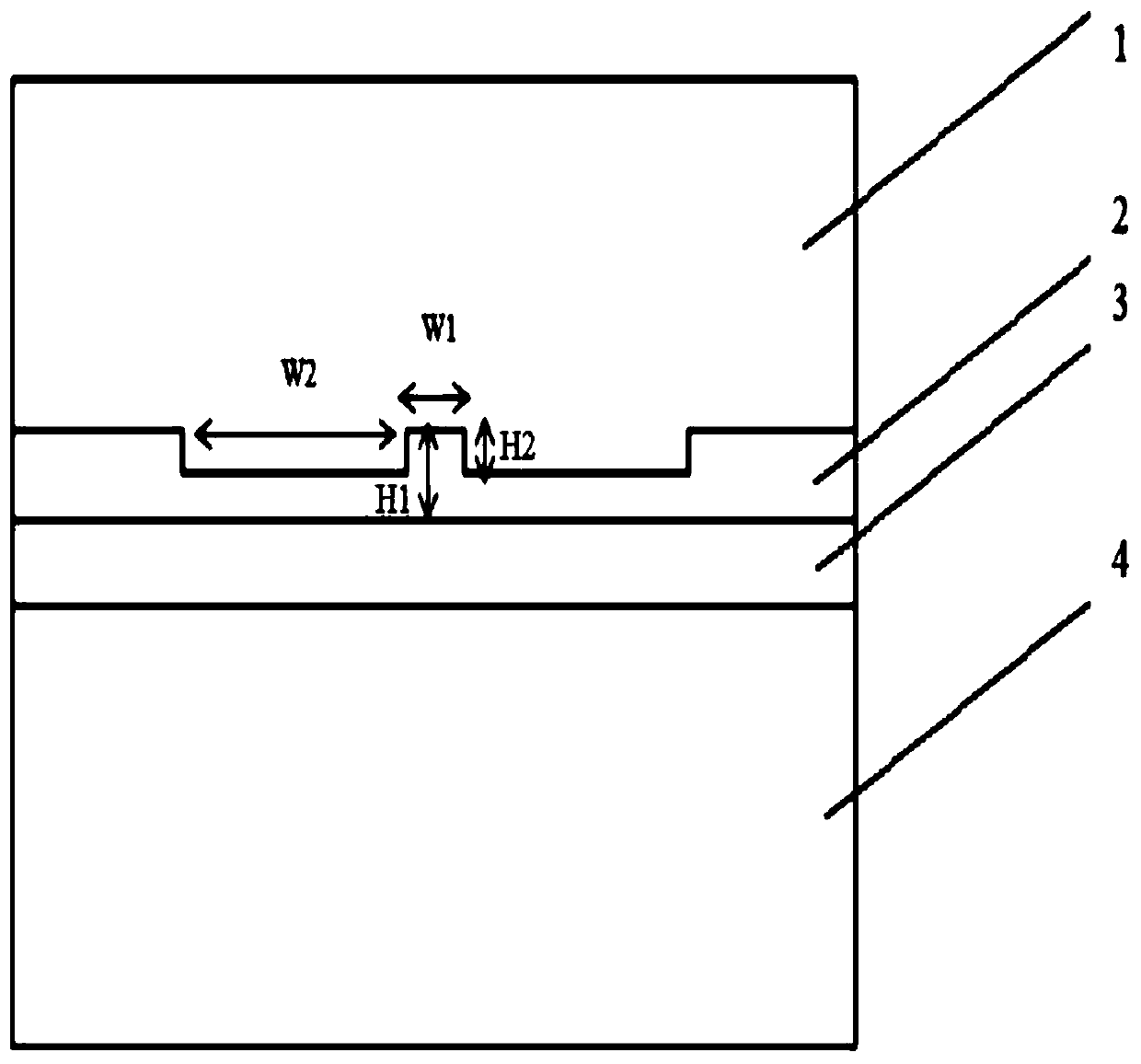
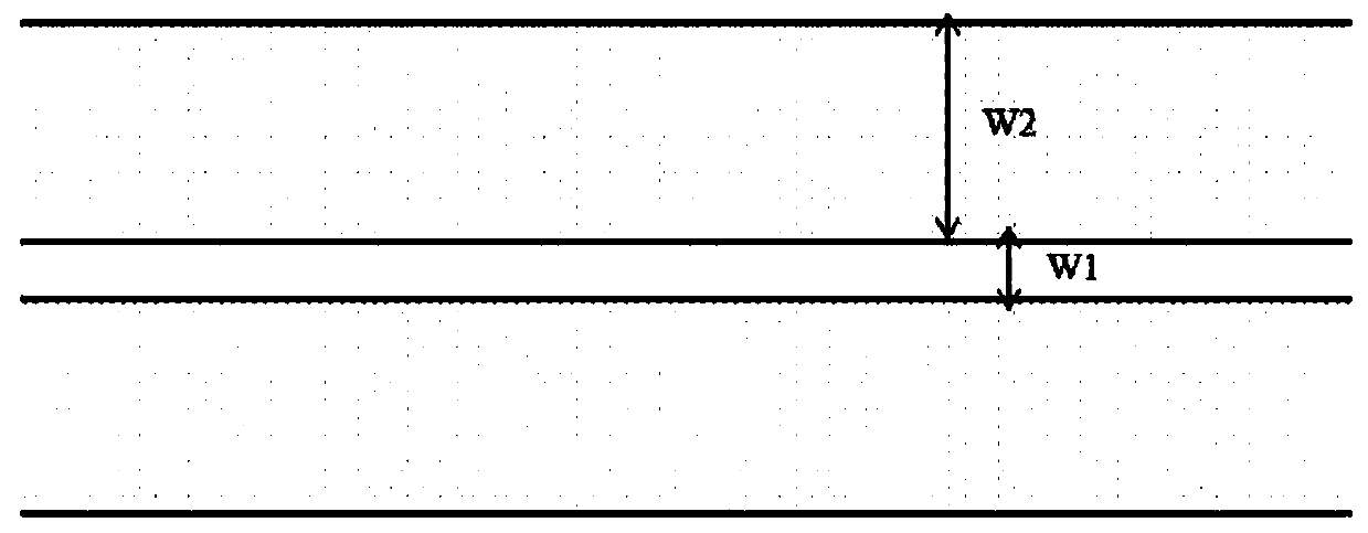
[0033] Figure 1-2 Shown is a schematic structural view of the thin-film lithium niobate single-polarization waveguide of this embodiment. The thin-film lithium niobate single-polarization waveguide of this embodiment comprises a silicon nitride upper cladding layer 1, a thin-film lithium niobate waveguide core layer 2, a silicon dioxide lower cladding layer 3 and Quartz substrate 4. The main structure of this embodiment is an X-cut Y-pass thin-film lithium niobate ridge waveguide. Preferably, the entire single polarization optical circuit adopts the same single polarization waveguide design.
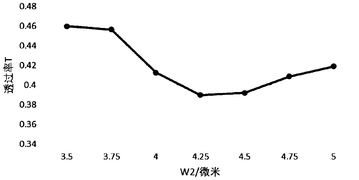
[0034] The ridge width W1 and etching depth H2 of the thin-film lithium niobate waveguide core layer are determined by FDE simulation, and the widths of the grooves on both sides of the waveguide are determined by FDTD simulation. The total thickness H1 of the lithium niobate thin film is a fixed value. When the width W1 and the etching depth H2 are smaller than their theoretical ma...
Embodiment 2
[0044] The structural schematic diagram of the thin-film lithium niobate single-polarization waveguide of this embodiment can still refer to Figure 1-2 . The thin-film lithium niobate single-polarization waveguide of this embodiment includes a silicon dioxide upper cladding layer, a thin-film lithium niobate ridge waveguide core layer, a silicon dioxide lower cladding layer, and a silicon substrate. The main structure of this embodiment is an X-cut Y-pass thin-film lithium niobate ridge waveguide.
[0045] The preparation method of the thin-film lithium niobate single-polarization ridge waveguide of this embodiment comprises the following steps:
[0046] S1. Prepare thin film lithium niobate on insulator (Lithium niobate on insulator, LNOI);
[0047] S2: Cover a layer of metal material with conventional EBE (Electron Beam Evaporation, EBE) on the lithium niobate film, and expose the groove-shaped areas on both sides of the ridge-shaped waveguide protrusion structure on the...
PUM
| Property | Measurement | Unit |
|---|---|---|
| width | aaaaa | aaaaa |
| depth | aaaaa | aaaaa |
| width | aaaaa | aaaaa |
Abstract
Description
Claims
Application Information


