Low-profile broadband microstrip antenna based on metasurface

A technology of microstrip antenna and metasurface, which is applied in the direction of antenna, antenna coupling, antenna components, etc., can solve the problems affecting the quality of communication, and the conventional antenna cannot fully meet the requirements of modern communication, so as to solve the interference problems such as coupling and easy to carry Conformal, the effect of reducing the number of installations

Pending Publication Date: 2020-04-10
湖南国科锐承电子科技有限公司
View PDF0 Cites 6 Cited by
  • Summary
  • Abstract
  • Description
  • Claims
  • Application Information

AI Technical Summary

Problems solved by technology

[0002] With the rapid development of wireless communication system technology, the requirements for antenna performance are also increasing, and conventional antennas can no longer fully meet the requirements of modern communication.
In modern communication, it is necessary to equip more communication devices in the same space, so the number of antennas needs to be increased accordingly, so that the coupling between antennas directly affects the electrical indicators of the antennas, which ultimately affects the communication quality; therefore, a Antennas meet higher transmission performance

Method used


Image

  • Low-profile broadband microstrip antenna based on metasurface
  • Low-profile broadband microstrip antenna based on metasurface
  • Low-profile broadband microstrip antenna based on metasurface

Examples


Embodiment 1

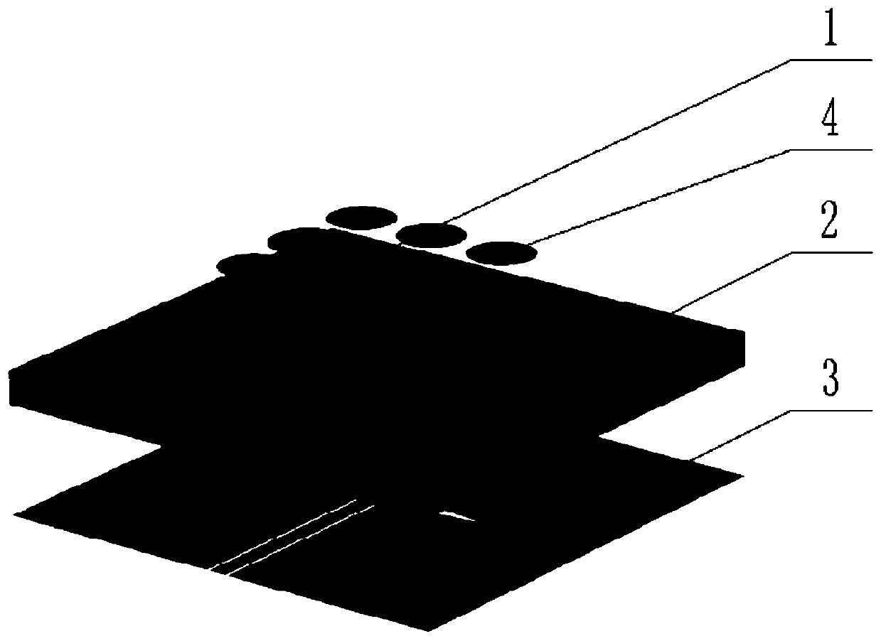
[0034] Embodiment 1: a kind of low profile broadband microstrip antenna based on metasurface, such as figure 1 As shown; including metasurface radiation layer 1, dielectric substrate layer 2 and feed layer 3 arranged in sequence from top to bottom; metasurface radiation layer 1 is mounted on the upper end of dielectric substrate layer 2, and feed layer 3 is mounted on the dielectric The lower end of the substrate layer 2; the metasurface radiation layer 1 contains nine circular radiation elements 4; the feed layer 3 includes CPW feeders 5, triangular metal branches 6, gradual coupling slots 7 and metal floor 8; the signal is input from the CPW feeder 5 , the signal is coupled to the metasurface radiation layer 1 through the triangular metal branch 6 and the gradual coupling gap 7, thereby forming a wider impedance bandwidth. The antenna adopts printed circuit board technology, in which the material of the radiation layer 1 and the feed layer 3 is metal copper, and the material...

Embodiment 2

[0039] Embodiment 2: the difference between this embodiment and embodiment 1 is:

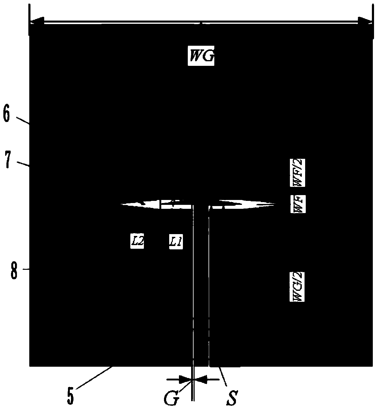
[0040] The width S of the CPW feeder 5 is 1.5 mm. The feeder extends to the center of the plane and connects with the metal floor 8 to form a short circuit. The gap g between the feeder and the metal floor 8 is 0.2 mm. The triangular metal branch 6 is left-right symmetrical and directly connected to the feeder. The length L1 of the long right-angle side is 3mm, and the distance WF / 2 between it and the metal floor 8 is 0.5mm; the gradient coupling gap 7 is located in the center of the entire plane, and the gradient distance L2 is 4mm, symmetrical up and down, and the widest width at the gradient For WF, the narrowest width is 0.

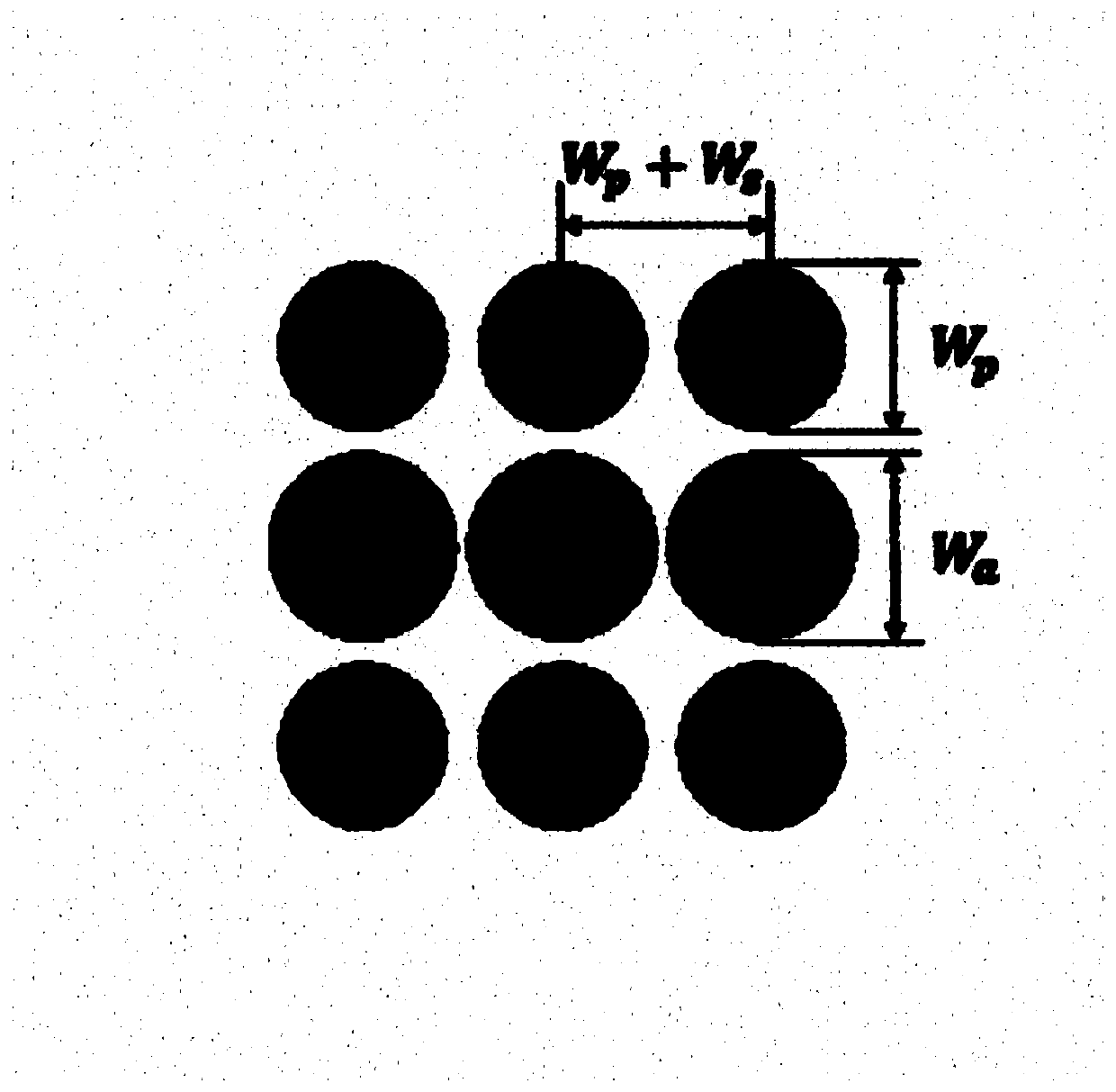
[0041] The distance between the centers of the upper and lower rows of adjacent circular radiation units 4 is a fixed value of 7mm, and the diameters of the upper, middle and lower rows of circular units are different. Among them, the diameter of the upper and lower row...

Embodiment 3

[0043] Embodiment 3: the difference between this embodiment and embodiment 1 is:

[0044] like figure 2 As shown: the width S of the CPW feeder 5 is 1.2mm, the feeder extends to the center of the plane and connects with the metal floor 8 to form a short circuit, the gap g between the feeder and the metal floor 8 is 0.3mm; The length L1 of its long right-angled side is 2.8mm, and the distance WF / 2 between it and the metal floor 8 is 0.6; the gradient coupling gap 7 is located in the center of the entire plane, and the gradient distance L2 is 3.7mm, which is symmetrical up and down and gradually The widest width is WF, and the narrowest width is 0.

[0045] like image 3 As shown, the 3x 3 circular radiation unit 4 is composed of a regular metasurface structure, the distance Wp+Ws between the centers of the upper and lower rows of adjacent circular radiation units 4 is a fixed value of 6.5mm, and the upper, middle and lower rows of circular units The diameters are different....


PUM


Abstract

The invention discloses a low-profile broadband microstrip antenna based on a metasurface. The low-profile broadband microstrip antenna comprises a metasurface radiation layer, a dielectric substratelayer and a feed layer which are sequentially arranged from top to bottom, the metasurface radiation layer is attached to the upper layer of the dielectric substrate, and the feed layer is attached tothe lower layer of the dielectric substrate. The metasurface radiation layer comprises nine circular radiation units. The feed layer comprises a CPW feed line, a triangular metal branch, a gradual change type coupling gap and a metal floor. Signals are input through the CPW feed line and are coupled to the metasurface radiation layer through the triangular metal branch and the gradual change typecoupling gaps, and therefore a wide impedance bandwidth is formed. By adopting the metasurface structure taking a circular patch as a radiation unit, the impedance bandwidth of the whole antenna is improved, and the directivity of the high-frequency-band antenna is ensured. A gradual change type coupling feed structure is adopted, and compared with coupling feed of the CPW feed line, the gradualchange type structure can greatly improve the impedance bandwidth of the antenna and can reduce the profile of the antenna.

Description

technical field [0001] The invention relates to the technical field of X-band antennas, in particular to a low-profile broadband metasurface microstrip antenna. Background technique [0002] With the rapid development of wireless communication system technology, the requirements for antenna performance are also increasing, and conventional antennas can no longer fully meet the requirements of modern communication. In modern communication, it is necessary to equip more communication devices in the same space, so the number of antennas needs to be increased accordingly, so that the coupling between antennas directly affects the electrical indicators of the antennas, which ultimately affects the communication quality; therefore, a This antenna satisfies higher transmission performance. Contents of the invention [0003] The present invention proposes a broadband low-profile metasurface antenna, which has the characteristics of wide frequency bandwidth, low profile, miniaturi...

Claims


Application Information

Patent Timeline
Patent Type & Authority Applications(China)
IPC IPC(8): H01Q1/38H01Q1/50H01Q1/52H01Q1/48
CPCH01Q1/38H01Q1/48H01Q1/50H01Q1/521
Inventor 朱江文建森杨军杨虎姜南
Owner 湖南国科锐承电子科技有限公司
Why Eureka
Try Eureka