System and method for testing point source transmittance of optical device

A point source transmittance, optical device technology, applied in the field of optical detection, can solve the problems of high electronic control requirements, bulky equipment, and narrow test dynamic range.

Pending Publication Date: 2020-04-17
NO 34 RES INST OF CHINA ELECTRONICS TECH GRP
View PDF0 Cites 3 Cited by
  • Summary
  • Abstract
  • Description
  • Claims
  • Application Information

AI Technical Summary

Problems solved by technology

This test method requires precise turntable and high electronic control requirements, and the equipment is bulky, which is not conducive to the promotion of engineering applications; the existing test equipment has a complicated way to generate uniformly distributed parallel light; the fixed wavelength of the collimator light source cannot take into account visible light to near-infrared or even In the mid-to-far infrared band; the test dynamic range is narrow, and it cannot take into account the measurement of stray light power from large angles to the edge of the field of view

Method used


Image

  • System and method for testing point source transmittance of optical device
  • System and method for testing point source transmittance of optical device
  • System and method for testing point source transmittance of optical device

Examples


Embodiment Construction

[0056] In order to make the technical solution of the present invention clearer, the present invention will be further described in detail below in conjunction with the accompanying drawings.

[0057] Embodiment of Point Source Transmittance Testing System for Optical Devices

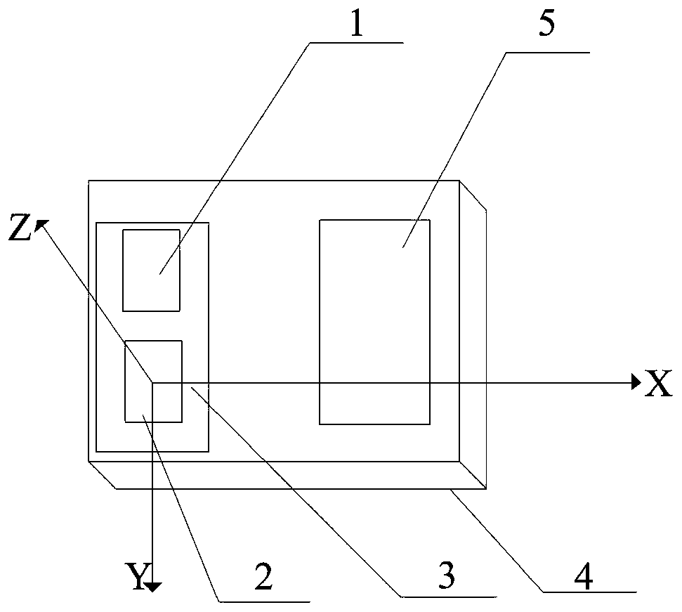
[0058] The overall structure schematic diagram of the embodiment of the point source transmittance test system of the optical device is as follows figure 1 As shown, it includes a support structure 4, a collimator 5, a two-dimensional turntable 3 and a photoelectric theodolite 1. The installation horizontal plane of the support structure 4 is the X and Y planes, and the collimator 5 is fixed on the support structure 4 at one end of the X axis. The output light is along the X-axis direction of the support structure 4; the two-dimensional turntable 3 is installed on the other end of the X-axis on the support structure 4, and the two-dimensional turntable 3 is equipped with a manual thread adjustment mecha...


PUM


Abstract

The invention relates to a system and a method for testing the transmittance of a point source of an optical device. A collimator is fixed at one end of an X-axis of a support structure of the system,a two-dimensional rotary disc is mounted at the other end of the X-axis of the support structure, and a photoelectric theodolite and a to-be-measured optical device are mounted on the two-dimensionalrotary disc. The testing method comprises steps of adjusting a two-dimensional rotary disc to enable an optical axis of an optical device to be parallel to collimator beams, and measuring an opticalpower value at an entrance pupil of the optical device; adjusting the attenuation amount of an optical attenuator; adjusting the photoelectric theodolite to enable the center of the flat-topped optical fiber in the field of view of the telescope to be located in the center of a cross wire; the photoelectric theodolite rotates by theta 1, the two-dimensional rotary disc rotates by -theta 1, the center of the flat-topped optical fiber in the field of view is located in the center of the cross wire again, an optical power value is recorded, and the point source transmittance PST (theta 1) of theto-be-measured optical device at the moment is calculated; the rotation angle of the photoelectric theodolite is continuously adjusted to obtain a series of theta i and PST (theta i), and a PST curveis drawn. The method is advantaged in that the method improves the dynamic range of point source transmittance measurement, and is simple in principle, convenient to operate and easy to implement.

Description

technical field [0001] The invention relates to the field of optical detection, in particular to a point source transmittance test system and a test method of an optical device. Background technique [0002] In a wireless optical communication system, in order to realize the establishment of a long-distance communication link, it usually starts from three aspects, that is, reducing the divergence angle at the transmitting end, increasing the receiving aperture at the receiving end, and increasing the sensitivity of the photodetector. In practical applications, due to the existence of diffraction limit and tracking accuracy, the reduction of the divergence angle of the emitted beam is limited. Due to the limitation of the manufacturing process of the large-aperture objective lens, the requirements of equipment volume, weight and power consumption of the turntable, the aperture of the receiving objective lens cannot be continuously increased. The design of highly sensitive de...

Claims


Application Information

Patent Timeline
IPC IPC(8): G01M11/02
CPCG01M11/02
Inventor 马拥华孙晖杨乾远刘金标蒋相刘学周远文
Owner NO 34 RES INST OF CHINA ELECTRONICS TECH GRP
Why Eureka
Try Eureka