E-fuse fusing characteristic test circuit and method

A test circuit and characteristic test technology, which is applied in the direction of measuring electricity, fuse testing, and measuring electrical variables, etc., can solve the problem of test chip area consumption, etc., and achieve the effect of saving test chip area, reducing area occupation, and improving area utilization.

Pending Publication Date: 2020-04-17
SEMITRONIX
View PDF0 Cites 2 Cited by
  • Summary
  • Abstract
  • Description
  • Claims
  • Application Information

AI Technical Summary

Problems solved by technology

Such a test method measures very few DUTs, and the area of ​​the test chip is seriously consumed.

Method used


Image

  • E-fuse fusing characteristic test circuit and method
  • E-fuse fusing characteristic test circuit and method
  • E-fuse fusing characteristic test circuit and method

Examples


Embodiment Construction

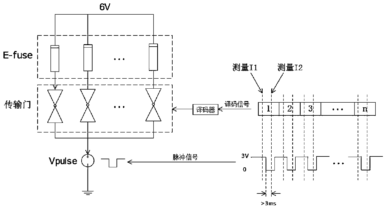
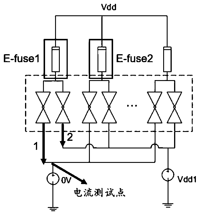
[0034] The following description serves to disclose the present invention to enable those skilled in the art to carry out the present invention. The preferred embodiments described below are only examples, and those skilled in the art can devise other obvious variations. The basic principles of the present invention defined in the following description can be applied to other embodiments, variations, improvements, equivalents and other technical solutions without departing from the spirit and scope of the present invention.

[0035] Those skilled in the art should understand that, in the disclosure of the present invention, the terms "vertical", "transverse", "upper", "lower", "front", "rear", "left", "right", " The orientation or positional relationship indicated by "vertical", "horizontal", "top", "bottom", "inner", "outer", etc. is based on the orientation or positional relationship shown in the drawings, which are only for the convenience of describing the present inventio...


PUM


Abstract

The invention provides an E-fuse fusing characteristic test circuit. The E-fuse fusing characteristic test circuit comprises a switch controller, a voltage source, at least one to-be-tested E-fuse anda switch module, the output end of the switch control module is connected to the switch module; wherein one end of each to-be-tested E-fuse is connected to a fixed potential end, the other end of each to-be-tested E-fuse is connected to the voltage source, and each to-be-tested E-fuse is connected with the switch module and used for controlling on-off of a test circuit where the to-be-tested E-fuse is located through the switch module; according to the test circuit, the number of DUTs capable of being tested is greatly increased, the area of a test chip is saved, meanwhile, a fusing voltage and a non-fusing voltage are adopted for testing, and whether E-fuse fusing is caused by testing or not can be judged; when a pulse voltage test signal is adopted, the hidden danger of current accumulation caused by E-fuse test of a traditional addressable test structure is avoided, and the area occupation of a peripheral test circuit can be further reduced.

Description

technical field [0001] The invention relates to the technical field of chip testing, in particular to a test circuit and a test method for E-fuse fusing characteristics. Background technique [0002] Fuse (fuse) has always been used to guide the electronic signal in the chip. It is a key element to realize the repair technology. The difference between the resistance before and after the fuse is blown is used to change the connection relationship of the original circuit, so that the failed memory unit can be replaced by Redundancy Cells. Replacement, in order to achieve the purpose of repairing the failed memory cell array and improving the yield rate of the chip. Traditionally, most chip manufacturers have adopted Laser-fuse (laser fusing) technology, that is, the fuse is fused by emitting a laser with a certain energy and time. However, with the miniaturization of the manufacturing process, Laser-fuse occupies a large amount of chip area, and its size cannot be reduced wit...

Claims


Application Information

Patent Timeline
Patent Type & Authority Applications(China)
IPC IPC(8): G01R31/74G01R31/28
CPCG01R31/2853
Inventor 刘禹延吕圣凯杨璐丹方益
Owner SEMITRONIX
Why Eureka
Try Eureka